


 A Ti/Cu fémbevonatú szilíciumszeletet szabványos vezető és folyamat-kompatibilis szubsztrátként tervezték a fejlett kutatási és ipari alkalmazásokhoz. A szilícium ostyatechnológia és a fém vékonyréteg bevonat kombinálásával stabil platformot biztosít elektromos, kémiai és mikrogyártási folyamatokhoz.
A Ti/Cu bevonatrendszer szerkezete egyszerre biztosítja a mechanikai megbízhatóságot és a funkcionális vezetőképességet. Különösen alkalmas olyan alkalmazásokhoz, amelyek megbízható fémfelületeket, egyenletes felületi vezetőképességet és a szabványos félvezető-feldolgozási technikákkal való kompatibilitást igényelnek.
A termék támogatja az ostyaméret, a hordozó típusa és a filmvastagság testreszabását, így alkalmas mind a kisléptékű kutatási kísérletekhez, mind a kísérleti gyártási környezetekhez.
 Fő jellemzők
- Erős tapadási teljesítmény
A titán tapadóréteg jelentősen javítja a rézfilm és a szilíciumszubsztrát közötti kötést, csökkentve a leválás és a leválás kockázatát. - Nagy elektromos vezetőképesség
A réz felületi réteg alacsony ellenállást és stabil elektromos teljesítményt biztosít az eszközök teszteléséhez és a vezető alkalmazásokhoz. - Kiváló filmegyenletesség
A magnetronos porlasztás egyenletes bevonatvastagságot és sima felületi morfológiát biztosít a teljes ostyán. - Jó folyamat-kompatibilitás
Kompatibilis a litográfiával, maratással, galvanizálással, leválasztással és a szokásos félvezetőgyártási eljárásokkal. - Rugalmas testreszabás
Többféle ostyaméretben, hordozótípusban és fémrétegvastagság-kombinációban kapható.
 Tipikus struktúra
Alátét + titán tapadó réteg + réz vezető réteg
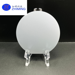
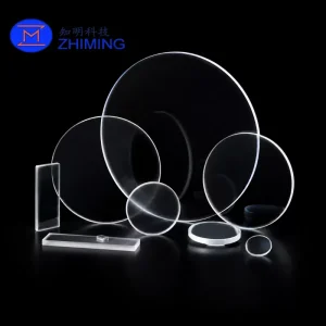
- Alátét: Szilícium / kvarc / üveg (opcionális)
- Tapadó réteg: Titán (Ti)
- Vezető réteg: Réz (Cu)
- Lerakási módszer: Magnetron porlasztás
A Ti réteg a hordozó és a rézfilm közötti határfelületi kötőrétegként működik, biztosítva a szerkezeti stabilitást. A Cu réteg biztosítja a funkcionális vezető felületet az elektromos és technológiai alkalmazásokhoz.
Műszaki adatok
| Tétel | Leírás |
|---|---|
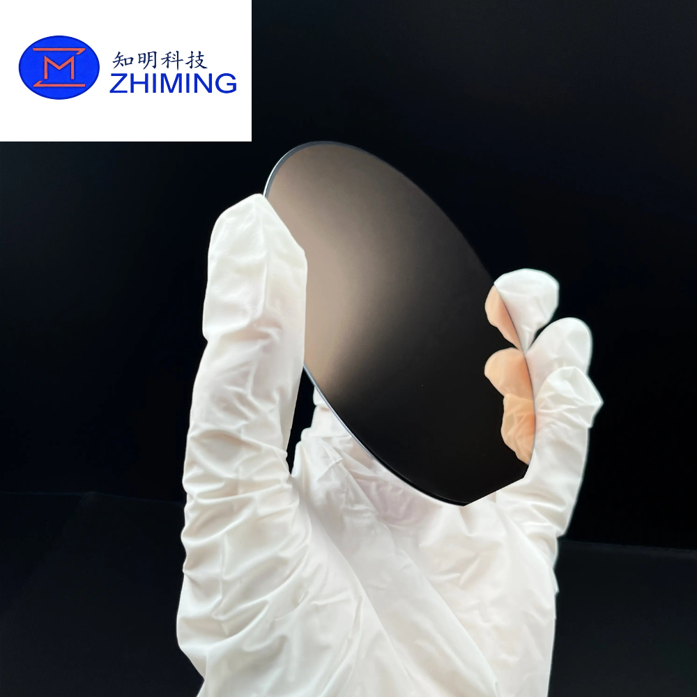
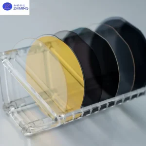
| Wafer méret | 2″, 4″, 6″, 8″, egyedi méretben |
| Alátét Anyag | Szilícium, kvarc, BF33 üveg (opcionális) |
| Kristály orientáció | , stb. |
| Ellenállás | Alacsony / Közepes / Magas (testreszabható) |
| Ti vastagság | 10-50 nm (tipikus tartomány) |
| Cu vastagság | 50 nm - 1 µm (porlasztva), vastagabb galvanizálással |
| Bevonási módszer | Magnetron porlasztás |
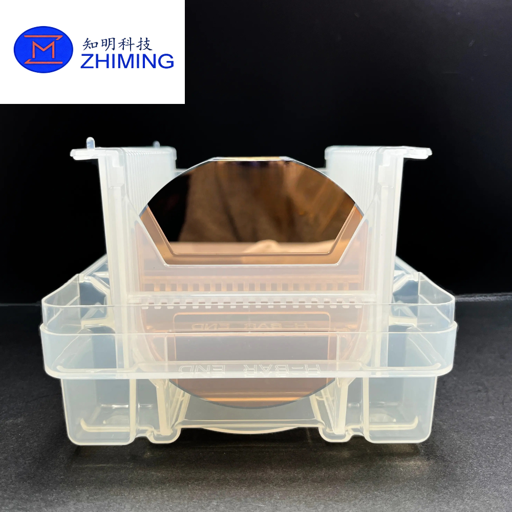
| Bevonat oldal | Egyoldalas vagy kétoldalas |
 Gyártási folyamat
A Ti/Cu fémbevonatú ostyát vákuum magnetronporlasztásos technológiával állítják elő. Először egy titánréteget helyeznek el a megtisztított szilíciumfelületen a tapadás javítása érdekében. Ezután a titánréteg tetejére egy rézréteg kerül, hogy egységes vezető felületet képezzen.
A vastagabb rézrétegeket igénylő alkalmazások esetében a porlasztott rézréteg galvanizáláshoz magvető rétegként használható, ami további fémnövekedést tesz lehetővé a mikronos vastagság elérése érdekében, miközben erős tapadást biztosít.
Ez a kombinált eljárás egyszerre biztosítja a magas filmminőséget és a rugalmas funkcionális terjeszkedést.
Alkalmazások
- Félvezető eszközök kutatása és prototípusgyártás
- Ohmos érintkezés és elektródagyártás
- MEMS mikroszerkezetű csíraréteg fejlesztése
- Galvanizáló alap RDL és vastag rézszerkezetekhez
- Vékonyfilmek és nanoanyagok növekedésének kutatása
- Felületi vezetőképesség vizsgálata és anyagelemzés
- SEM, AFM és felületi metrológiai mintaelőkészítés
- Bio-elektrokémiai érzékelők és microarray platformok
Előnyök az egyszerű fémbevonattal szemben
A szilíciumra történő közvetlen rézbevonattal összehasonlítva a Ti/Cu szerkezet:
- Jobb tapadási stabilitás termikus és kémiai igénybevétel esetén
- A réz hámlásának vagy repedezésének csökkent kockázata
- Javított folyamathozam a mikrogyártási lépésekben
- Idővel stabilabb elektromos teljesítmény
- Jobb kompatibilitás a többlépcsős félvezető eljárásokkal
Ez megbízhatóbb megoldást jelent mind a kutatólaboratóriumok, mind az ipari K+F környezetek számára.
GYIK
1. kérdés: Miért használnak titániumot rézbevonat alatt?
A titán adhéziós rétegként működik, amely javítja a réz és a szilícium szubsztrátumok közötti kötést, megakadályozva a leválást a feldolgozás és a használat során.
2. kérdés: Lehet-e növelni a réz vastagságát?
Igen. A porlasztott réz felhasználható galvanizáló rétegként, hogy az alkalmazás követelményeitől függően vastagabb fémrétegeket érjen el.
3. kérdés: Az ostya mindkét oldala bevonható?
Igen. Kérésre egy- vagy kétoldalas bevonási lehetőség is rendelkezésre áll.
4. kérdés: Milyen szubsztrát lehetőségek állnak rendelkezésre?
A leggyakoribb a szabványos szilícium, de speciális optikai vagy kémiai alkalmazásokhoz kvarc és üveg szubsztrátumok is rendelkezésre állnak.

Értékelések
Még nincsenek értékelések.