

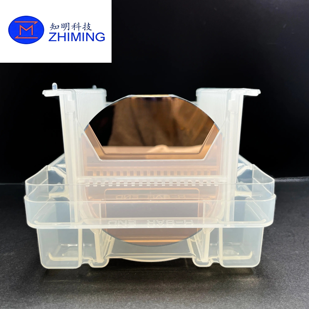
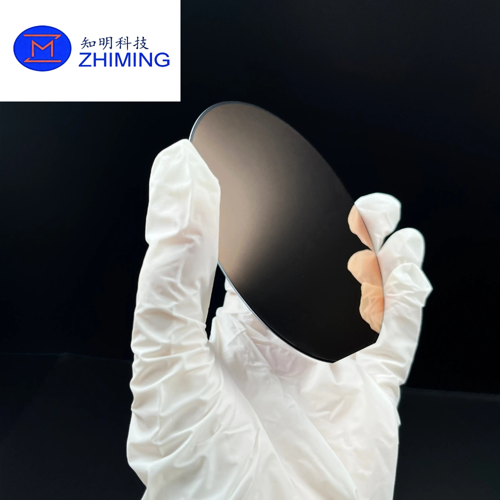

 Ti/Cu Metal-Coated Silicon Wafer ist als leitfähiges und prozesskompatibles Standardsubstrat für fortgeschrittene Forschungs- und Industrieanwendungen konzipiert. Durch die Kombination der Silizium-Wafer-Technologie mit einer Metall-Dünnfilmbeschichtung bietet es eine stabile Plattform für elektrische, chemische und mikrotechnische Prozesse.
Die Struktur des Ti/Cu-Beschichtungssystems gewährleistet sowohl mechanische Zuverlässigkeit als auch funktionale Leitfähigkeit. Es eignet sich besonders für Anwendungen, die zuverlässige Metallschnittstellen, gleichmäßige Oberflächenleitfähigkeit und Kompatibilität mit Standard-Halbleiterverarbeitungstechniken erfordern.
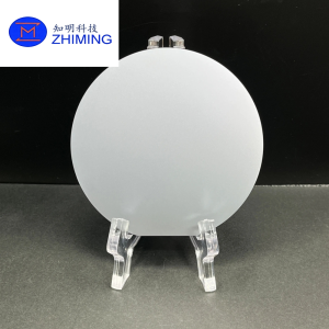
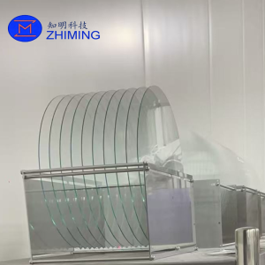
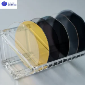
Das Produkt kann in Bezug auf Wafergröße, Substrattyp und Schichtdicke individuell angepasst werden und eignet sich daher sowohl für kleine Forschungsexperimente als auch für Pilotproduktionsumgebungen.
 Wesentliche Merkmale
- Starke Klebeleistung
Die Haftschicht aus Titan verbessert die Haftung zwischen der Kupferfolie und dem Siliziumsubstrat erheblich und verringert das Risiko von Ablösungen und Delaminationen. - Hohe elektrische Leitfähigkeit
Die Oberflächenschicht aus Kupfer bietet einen geringen Widerstand und eine stabile elektrische Leistung für Gerätetests und leitfähige Anwendungen. - Ausgezeichnete Gleichmäßigkeit des Films
Die Magnetronzerstäubung gewährleistet eine gleichmäßige Schichtdicke und eine glatte Oberflächenmorphologie auf dem gesamten Wafer. - Gute Prozesskompatibilität
Kompatibel mit Lithografie, Ätzen, Galvanik, Abscheidung und Standard-Halbleiterherstellungsprozessen. - Flexible Anpassung
Erhältlich in verschiedenen Wafergrößen, Substrattypen und Metallschichtdickenkombinationen.
 Typische Struktur
Substrat + Titan-Haftschicht + Kupfer-Leitschicht
- Trägermaterial: Silizium / Quarz / Glas (optional)
- Adhäsionsschicht: Titan (Ti)
- Leitende Schicht: Kupfer (Cu)
- Abscheidungsmethode: Magnetronzerstäubung
Die Ti-Schicht fungiert als Verbindungsschicht zwischen dem Substrat und dem Kupferfilm und sorgt für strukturelle Stabilität. Die Cu-Schicht bildet die funktionale leitfähige Oberfläche für elektrische und verfahrenstechnische Anwendungen.
Spezifikationen
| Artikel | Beschreibung |
|---|---|
| Wafer Größe | 2″, 4″, 6″, 8″, Sondergrößen |
| Material des Substrats | Silizium, Quarz, BF33-Glas (optional) |
| Kristall-Ausrichtung | , , usw. |
| Widerstandsfähigkeit | Niedrig / Mittel / Hoch (anpassbar) |
| Ti-Dicke | 10-50 nm (typischer Bereich) |
| Cu-Dicke | 50 nm - 1 µm (gesputtert), dicker durch galvanische Abscheidung |
| Beschichtungsmethode | Magnetronzerstäubung |
| Beschichtung Seite | Einseitig oder doppelseitig |
 Herstellungsprozess
Der mit Ti/Cu-Metall beschichtete Wafer wird mit Hilfe der Vakuum-Magnetron-Sputter-Technologie hergestellt. Zunächst wird eine Titanschicht auf die gereinigte Siliziumoberfläche aufgebracht, um die Haftung zu verbessern. Dann wird eine Kupferschicht auf die Titanschicht aufgebracht, um eine einheitliche leitfähige Oberfläche zu bilden.
Für Anwendungen, die dickere Kupferschichten erfordern, kann die gesputterte Kupferschicht als Keimschicht für die Galvanisierung verwendet werden, die ein weiteres Metallwachstum ermöglicht, um eine Dicke im Mikrometerbereich zu erreichen und gleichzeitig eine starke Haftung zu gewährleisten.
Dieses Kombinationsverfahren gewährleistet sowohl eine hohe Folienqualität als auch eine flexible Funktionserweiterung.
Anwendungen
- Forschung und Prototyping von Halbleiterbauelementen
- Herstellung von ohmschen Kontakten und Elektroden
- Entwicklung einer MEMS-Mikrostruktur-Keimschicht
- Galvanische Basis für RDL und dicke Kupferstrukturen
- Forschung zum Wachstum von Dünnschichten und Nanomaterialien
- Prüfung der Oberflächenleitfähigkeit und Materialanalyse
- Probenvorbereitung für SEM, AFM und Oberflächenmetrologie
- Bio-elektrochemische Sensoren und Microarray-Plattformen
Vorteile im Vergleich zur einfachen Metallbeschichtung
Im Vergleich zur direkten Kupferbeschichtung auf Silizium bietet die Ti/Cu-Struktur:
- Bessere Adhäsionsstabilität bei thermischer und chemischer Belastung
- Geringeres Risiko, dass Kupfer abblättert oder Risse bekommt
- Verbesserte Prozessausbeute bei Mikrofabrikationsschritten
- Stabilere elektrische Leistung im Laufe der Zeit
- Bessere Kompatibilität mit mehrstufigen Halbleiterprozessen
Dies macht es zu einer zuverlässigeren Lösung sowohl für Forschungslabors als auch für industrielle F&E-Umgebungen.
FAQ
F1: Warum wird Titan unter einer Kupferbeschichtung verwendet?
Titan wirkt als Haftschicht, die die Verbindung zwischen Kupfer- und Siliziumsubstraten verbessert und eine Delaminierung während der Verarbeitung und Verwendung verhindert.
F2: Kann die Kupferdicke erhöht werden?
Ja, gesputtertes Kupfer kann als Keimschicht für die Galvanisierung verwendet werden, um je nach Anwendungsanforderungen dickere Metallschichten zu erzielen.
F3: Können beide Seiten des Wafers beschichtet werden?
Ja, einseitige oder beidseitige Beschichtung ist auf Anfrage möglich.
F4: Welche Substratoptionen gibt es?
Standard-Silizium ist am gebräuchlichsten, aber auch Quarz- und Glassubstrate sind für spezielle optische oder chemische Anwendungen erhältlich.

Rezensionen
Es gibt noch keine Rezensionen.