
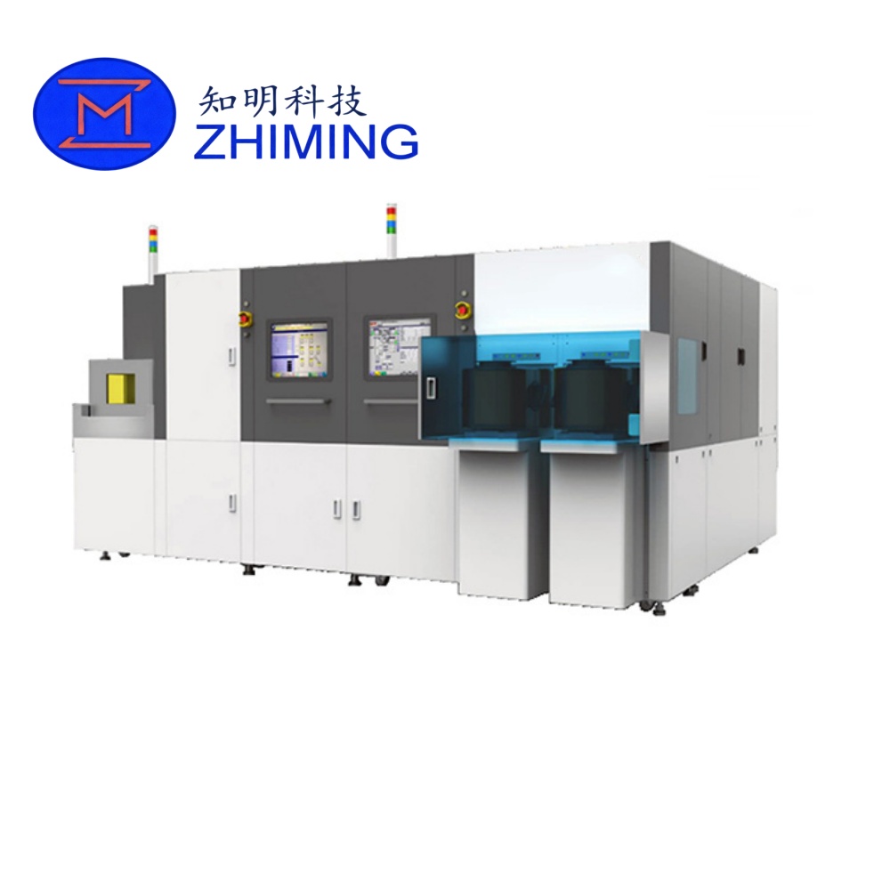
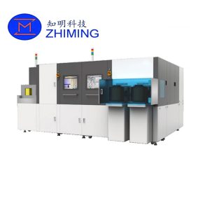
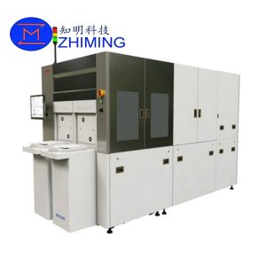
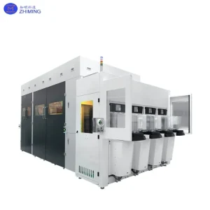
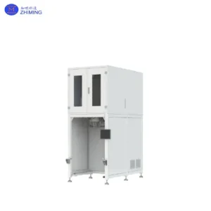
 The WGP-1271 Fully Automatic Wafer Thinning & Polishing Integrated Machine is a next-generation solution designed for ultra-thin wafer processing in advanced semiconductor packaging. By integrating grinding, polishing, cleaning, and tape handling into a single automated platform, the system significantly reduces process time while improving consistency and yield.
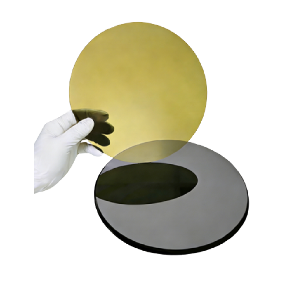
Engineered for wafers up to 300 mm (12 inches), the WGP-1271 enables stable thinning of wafers to below 50 μm, meeting the stringent requirements of advanced packaging technologies such as 3D IC, wafer-level packaging (WLP), and power device integration.
Unlike conventional multi-step systems, this machine combines back grinding and stress relief polishing into a unified process, minimizing wafer handling and reducing the risk of damage. The result is improved wafer integrity, higher throughput, and lower total cost of ownership (TCO).
Caraterísticas principais
1. Integrated Thinning and Polishing Process
The WGP-1271 combines coarse grinding, fine grinding, and polishing into a single workflow. This integrated design eliminates intermediate transfer steps, significantly reducing non-processing time and improving overall production efficiency.
2. Ultra-Thin Wafer Capability (<50 μm)
The system is specifically designed for ultra-thin wafer applications. It ensures stable processing and safe handling of wafers below 50 microns, which are typically fragile and prone to warpage or cracking.
3. Three-Spindle Four-Station Architecture
With a three-spindle, four-chuck configuration, the WGP-1271 enables parallel processing and high throughput. Each spindle is optimized for different stages of the process:
- Spindle 1: Coarse grinding
- Spindle 2: Fine grinding
- Spindle 3: Polishing / ultra-precision thinning (optional dry polishing)
This modular approach ensures both flexibility and precision.
4. Advanced In-Line Thickness Measurement (NCG + Auto TTV)
The system integrates Swing NCG (Non-Contact Gauge) with Auto TTV control, enabling real-time, non-contact wafer thickness measurement. This allows continuous monitoring and automatic adjustment of thickness uniformity throughout the process.
5. Fully Automated End-to-End Processing
The WGP-1271 supports a complete automated workflow, including:
- Grinding
- Polishing
- Wafer transfer
- Cleaning
- Tape mounting and removal
This reduces manual intervention, improves repeatability, and ensures compatibility with modern smart manufacturing environments.
6. Optional Dry Polishing & Ultra-Precision Grinding
The third spindle (Z3 axis) supports X-axis movement and can be configured for dry polishing or ultra-precision grinding, enabling diverse process applications depending on customer requirements.
 Aplicações
The WGP-1271 is ideal for advanced semiconductor manufacturing processes, including:
- Ultra-thin wafer processing (≤ 12 inch)
- Advanced packaging (WLP, Fan-out, 3D IC)
- IGBT and power semiconductor devices
- Silicon (Si) wafer thinning
- Silicon carbide (SiC) wafer processing
- High-density integrated circuit manufacturing
Its capability to handle ultra-thin wafers makes it particularly suitable for next-generation electronic devices requiring compact size and high performance.
Especificações técnicas
| Parâmetro | Especificação |
|---|---|
| Structure | 3 Spindles / 4 Chucks / 1 Workstation / Automatic Transfer & Cleaning System / Tape Mounting & Removal System |
| Tamanho da pastilha | 8 inch / 12 inch (Up to 300 mm) |
| Spindle Power | 7.5 kW / 11 kW (Optional) |
| Special Feature | Z3 Axis with X-axis movement |
| Processing Capability | Grinding + Polishing + Cleaning + Tape Handling |
| Minimum Thickness | < 50 μm |
| Dimensions (W×D×H) | 4050 × 3530 × 1900 mm |
Performance Advantages
Higher Efficiency
The integrated design reduces process steps and handling time, leading to significantly higher throughput compared to traditional separate systems.
Improved Yield
Non-contact measurement and low-stress processing minimize wafer damage, resulting in higher yield and better device reliability.
Superior Thickness Control
Real-time TTV adjustment ensures excellent thickness uniformity, which is critical for advanced packaging applications.
Reduced Risk of Contamination
Fewer transfer steps and a controlled process environment help maintain wafer cleanliness and reduce defect rates.
Enhanced Process Flexibility
Optional dry polishing and ultra-precision grinding allow customization for different materials and applications.
 Engineering Value & Industry Significance
As semiconductor devices continue to evolve toward higher performance and smaller form factors, ultra-thin wafers have become a critical requirement. However, thinning wafers below 50 μm introduces significant challenges in handling, stress control, and defect prevention.
The WGP-1271 addresses these challenges through integrated engineering design, combining multiple process steps into a single automated system. This not only improves production efficiency but also enhances process reliability, making it a valuable asset for semiconductor manufacturers transitioning to advanced packaging technologies.
FAQ
1. What is the main advantage of an integrated thinning and polishing system?
It reduces wafer handling steps, shortens processing time, and minimizes the risk of wafer damage, leading to higher efficiency and yield.
2. Can the WGP-1271 process ultra-thin wafers below 50 μm?
Yes, the system is specifically designed to handle and process wafers thinner than 50 μm with high stability and precision.
3. What types of wafers are supported?
The machine supports silicon (Si), silicon carbide (SiC), and other semiconductor wafers up to 300 mm.
4. How is thickness uniformity controlled?
Through an integrated non-contact measurement system (NCG) combined with Auto TTV adjustment for real-time control.
5. Does the machine support fully automated production?
Yes, it includes automatic transfer, cleaning, and tape handling systems, making it suitable for high-volume automated fabs.

Avaliações
Ainda não existem avaliações.