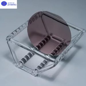
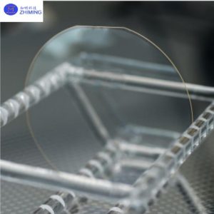
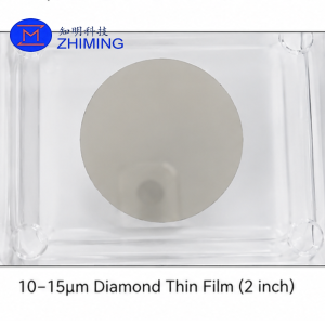
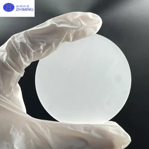
Thin-Film Lithium Niobate on Insulator LNOI Wafers for Integrated Photonic Applications

Thin-Film Lithium Niobate on Insulator (LNOI) wafers are advanced photonic substrates used for integrated optical, microwave photonic, and quantum systems.

The structure consists of a single-crystal lithium niobate thin film bonded onto a SiO₂ insulating layer and supported by a silicon substrate.

This configuration provides strong optical confinement, ultra-low propagation loss, and high electro-optic efficiency, making it a key platform for integrated photonics.

Thin-Film Lithium Niobate on Insulator LNOI Wafers for Integrated Photonic ApplicationsThin-Film Lithium Niobate on Insulator (LNOI) wafers are advanced photonic substrates used for integrated optical, microwave photonic, and quantum systems.

The structure consists of a single-crystal lithium niobate thin film bonded onto a SiO₂ insulating layer and supported by a silicon substrate.

This configuration provides strong optical confinement, ultra-low propagation loss, and high electro-optic efficiency, making it a key platform for integrated photonics.


What is Thin-Film Lithium Niobate (TFLN)

Thin-Film Lithium Niobate (TFLN) refers to a sub-micron crystalline LiNbO₃ layer engineered for optical waveguide and electro-optic applications.

Compared with bulk lithium niobate, TFLN enables tighter optical confinement, smaller device footprint, and higher integration density.

TFLN is typically implemented on LNOI wafers to form a complete integrated photonic platform.


Thin-Film Lithium Niobate on Insulator LNOI Wafers for Integrated Photonic Applications主要功能

  • Ultra-low optical loss < 0.05 dB/cm @ 1550 nm
  • High electro-optic coefficient (r₃₃ up to 90 pm/V)
  • Sub-micron waveguide compatibility (<1 μm)
  • CMOS-compatible integration with Si / SiN platforms
  • High thermal stability (~1140°C Curie temperature)
  • Multiple crystal cuts: X-cut / Y-cut / Z-cut
  • Wafer sizes: 3 inch / 4 inch / 6 inch / 8 inch

Wafer Structure

Layer 材質 Function
Top Layer LiNbO₃ Thin Film (TFLN) Electro-optic & nonlinear optical functionality
Middle Layer SiO₂ (Buried Oxide) Optical isolation & confinement
Bottom Layer Si / Quartz / Sapphire Mechanical support & CMOS compatibility

技術規格

Wafer Specifications

參數 價值
Wafer Diameter 3″, 4″, 6″, 8″
Total Thickness 525 ± 25 μm
弓形 ±50 μm
翹曲 <50 μm
LTV <1.5 μm (5×5 mm², 95%)

Thin-Film Lithium Niobate Layer

參數 價值
材質 Single-crystal LiNbO₃
厚度 300 nm – 1000 nm
Orientation Accuracy ±0.5°
表面粗糙度 Ra < 1 nm
Bonding Defects No defects >1 mm

Buried Oxide Layer (SiO₂)

參數 價值
材質 SiO₂
厚度 100 nm – 2 μm (customizable)
均一性 ±5%

Thin-Film Lithium Niobate on Insulator LNOI Wafers for Integrated Photonic ApplicationsFabrication Process

LNOI wafers are manufactured using semiconductor-grade processes:

  • Ion implantation for controlled layer separation
  • Wafer bonding onto insulating substrates
  • High-temperature annealing for crystal stabilization
  • Chemical Mechanical Polishing (CMP) for surface planarization
  • Final optical and structural quality inspection

Key Applications

  • High-speed optical communication (100G–800G modulators)
  • Quantum photonics (entangled photon generation, QKD systems)
  • Microwave photonics (RF signal processing, mmWave systems)
  • Nonlinear optics (frequency conversion, optical combs)
  • Integrated sensing systems (biochemical and optical resonators)

Performance Advantage vs Bulk LiNbO₃

財產 Bulk LiNbO₃ LNOI Thin Film
Optical Loss Higher <0.05 dB/cm
Integration High-density photonics
Device Size Large Sub-micron scale
CMOS Compatibility No Yes
Modulation Efficiency 中度 High (Vπ ~1V achievable)

客製化選項

Option 說明
Crystal Cut X-cut / Y-cut / Z-cut
薄膜厚度 300 nm – 1000 nm
Substrate Si / Quartz / Sapphire
Oxide Layer 100 nm – 2 μm (custom)
Doping MgO-doped LiNbO₃ available

品質控制

Test Item 方法
Optical Loss Waveguide propagation test
表面粗糙度 AFM measurement
厚度均勻性 Mapping system
Bonding Quality IR inspection
平整度 Wafer metrology

Engineering Capability

ZMSH provides full-process support for LNOI wafer development:

  • Thin-film design optimization
  • Wafer bonding process engineering
  • Photonic device fabrication support
  • Nanofabrication (EBL / IBE)
  • Optical performance testing and validation

Supports both R&D prototyping and scalable small-batch production up to 8-inch wafers.


常見問題

What is LNOI used for
LNOI wafers are widely used in optical communication, quantum photonics, nonlinear optics, and integrated photonic circuits.

What is the typical thin-film thickness
Typical lithium niobate thin-film thickness ranges from 300 nm to 1000 nm.

Why use LNOI instead of bulk lithium niobate
LNOI offers lower optical loss, higher integration density, and CMOS-compatible photonic integration.

Can LNOI integrate with silicon photonics
Yes, LNOI is fully compatible with silicon and silicon nitride photonic platforms.

商品評價

目前沒有評價。

搶先評價 “Thin-Film Lithium Niobate on Insulator LNOI Wafers for Integrated Photonic Applications”

發佈留言必須填寫的電子郵件地址不會公開。 必填欄位標示為 *