

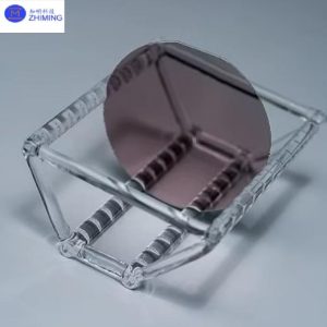
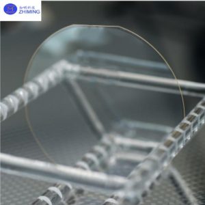
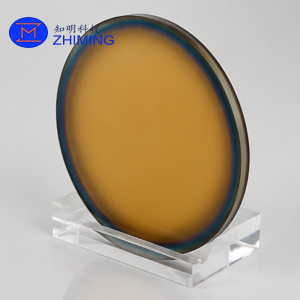
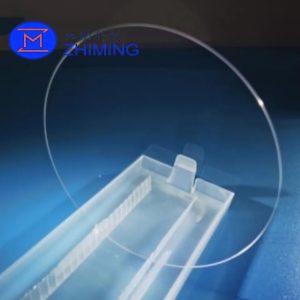
 Yalıtkan Üzerine İnce Film Lityum Niyobat (LNOI) yonga plakaları, entegre optik, mikrodalga fotonik ve kuantum sistemlerinde kullanılan gelişmiş fotonik alt tabakalardır.
Yapı, bir SiO₂ yalıtım tabakasına yapıştırılmış ve bir silikon alt tabaka üzerinde desteklenen tek kristal lityum niyobat ince tabakasından oluşmaktadır.
Bu yapı, güçlü optik sınırlama, son derece düşük iletim kaybı ve yüksek elektro-optik verimlilik sunarak entegre fotonik için önemli bir platform oluşturmaktadır.
İnce Film Lityum Niyobat (TFLN) nedir?
İnce Film Lityum Niyobat (TFLN), optik dalga kılavuzu ve elektro-optik uygulamalar için tasarlanmış, mikron altı boyutlarda bir kristal LiNbO₃ tabakasını ifade eder.
Toplu lityum niyobat ile karşılaştırıldığında, TFLN daha sıkı optik sınırlama, daha küçük cihaz boyutları ve daha yüksek entegrasyon yoğunluğu sağlar.
TFLN, genellikle eksiksiz bir entegre fotonik platform oluşturmak üzere LNOI yongaları üzerine uygulanır.
 Temel Özellikler
- 1550 nm'de < 0,05 dB/cm'lik ultra düşük optik kayıp
- Yüksek elektro-optik katsayı (r₃₃ 90 pm/V'ye kadar)
- Mikron altı dalga kılavuzu uyumluluğu (<1 μm)
- Si / SiN platformlarıyla CMOS uyumlu entegrasyon
- Yüksek termal kararlılık (~1140 °C Curie sıcaklığı)
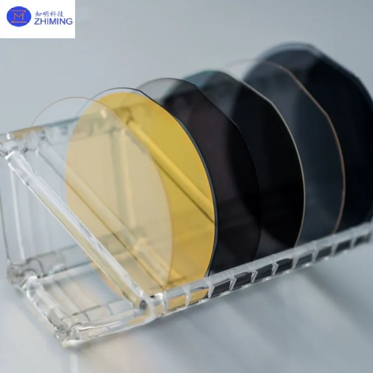
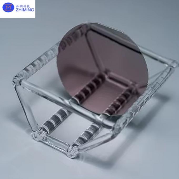
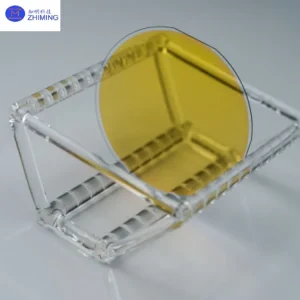
- Çeşitli kristal kesimleri: X kesimi / Y kesimi / Z kesimi
- Yonga boyutları: 3 inç / 4 inç / 6 inç / 8 inç
Yonga Yapısı
| Katman | Malzeme | İşlev |
|---|---|---|
| Üst Katman | LiNbO₃ İnce Film (TFLN) | Elektro-optik ve doğrusal olmayan optik işlevsellik |
| Orta Katman | SiO₂ (Gömülü Oksit) | Optik izolasyon ve sınırlama |
| Alt Katman | Silikon / Kuvars / Safir | Mekanik destek ve CMOS uyumluluğu |
Teknik Özellikler
Yonga Özellikleri
| Parametre | Değer |
|---|---|
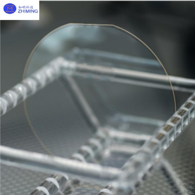
| Yonga Çapı | 3 inç, 4 inç, 6 inç, 8 inç |
| Toplam Kalınlık | 525 ± 25 μm |
| Yay | ±50 μm |
| Çözgü | <50 μm |
| LTV | <1,5 μm (5×5 mm², 95%) |
İnce Film Lityum Niyobat Katmanı
| Parametre | Değer |
|---|---|
| Malzeme | Tek kristal LiNbO₃ |
| Kalınlık | 300 nm – 1000 nm |
| Yön Doğruluğu | ±0,5° |
| Yüzey Pürüzlülüğü | Ra < 1 nm |
| Yapışma Kusurları | 1 mm'den büyük kusur yok |
Gömülü Oksit Katmanı (SiO₂)
| Parametre | Değer |
|---|---|
| Malzeme | SiO₂ |
| Kalınlık | 100 nm – 2 μm (isteğe göre ayarlanabilir) |
| Tekdüzelik | ±5% |
 Üretim Süreci
LNOI yonga plakaları, yarı iletken sınıfı üretim süreçleri kullanılarak üretilmektedir:
- Kontrollü tabaka ayrıştırma için iyon implantasyonu
- Yalıtkan alt tabakalara yonga yapıştırma
- Kristal stabilizasyonu için yüksek sıcaklıkta tavlama
- Yüzey düzleştirme için kimyasal-mekanik parlatma (CMP)
- Son optik ve yapısal kalite kontrolü
Başlıca Uygulamalar
- Yüksek hızlı optik iletişim (100G–800G modülatörler)
- Kuantum fotonik (dolaşık foton üretimi, QKD sistemleri)
- Mikrodalga fotoniği (RF sinyal işleme, mmWave sistemleri)
- Doğrusal olmayan optik (frekans dönüştürme, optik taraklar)
- Entegre algılama sistemleri (biyokimyasal ve optik rezonatörler)
Performans Avantajı ve Toplu LiNbO₃ Karşılaştırması
| Mülkiyet | Toplu LiNbO₃ | LNOI İnce Film |
|---|---|---|
| Optik Kayıp | Daha yüksek | <0,05 dB/cm |
| Entegrasyon | Düşük | Yüksek yoğunluklu fotonik |
| Cihaz Boyutu | Büyük | Mikron altı ölçek |
| CMOS Uyumluluğu | Hayır | Evet |
| Modülasyon Verimliliği | Orta düzeyde | Yüksek (Vπ ~1 V'ye ulaşılabilir) |
Özelleştirme Seçenekleri
| Seçenek | Açıklama |
|---|---|
| Kristal Kesim | X kesimi / Y kesimi / Z kesimi |
| Film Kalınlığı | 300 nm – 1000 nm |
| Alt tabaka | Silikon / Kuvars / Safir |
| Oksit Tabakası | 100 nm – 2 μm (isteğe göre) |
| Doping | MgO katkılı LiNbO₃ mevcuttur |
Kalite Kontrol
| Test Sorusu | Yöntem |
|---|---|
| Optik Kayıp | Dalga kılavuzu yayılım testi |
| Yüzey Pürüzlülüğü | AFM ölçümü |
| Kalınlık Tekdüzeliği | Haritalama sistemi |
| Yapışma Kalitesi | IR denetimi |
| Düzlük | Yonga metrologisi |
Mühendislik Yetkinliği
ZMSH LNOI yonga plakası geliştirme sürecinin tamamı boyunca destek sağlar:
- İnce film tasarım optimizasyonu
- Yonga birleştirme proses mühendisliği
- Fotonik cihaz üretimi desteği
- Nanofabrikasyon (EBL / IBE)
- Optik performans testi ve doğrulama
Hem Ar-Ge prototip üretimini hem de 8 inçlik yongalara kadar ölçeklenebilir küçük seri üretimi destekler.
SSS
LNOI ne için kullanılır?
LNOI yonga plakaları, optik iletişim, kuantum fotonik, doğrusal olmayan optik ve entegre fotonik devrelerde yaygın olarak kullanılmaktadır.
Tipik ince film kalınlığı nedir?
Tipik lityum niyobat ince film kalınlığı 300 nm ile 1000 nm arasında değişmektedir.
Neden toplu lityum niyobat yerine LNOI kullanılmalı?
LNOI, daha düşük optik kayıp, daha yüksek entegrasyon yoğunluğu ve CMOS ile uyumlu fotonik entegrasyon sunar.
LNOI, silikon fotonik ile entegre edilebilir mi?
Evet, LNOI silikon ve silikon nitrür fotonik platformlarla tam uyumludur.

Değerlendirmeler
Henüz değerlendirme yapılmadı.