

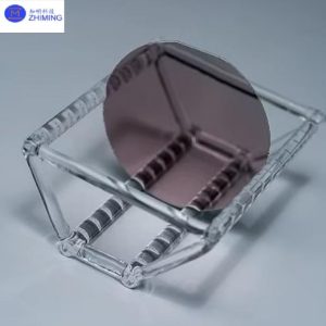
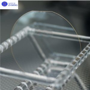
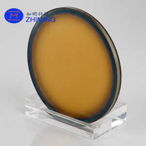
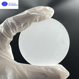
 Dünnschicht-LNOI-Wafer (Lithium-Niobat auf Isolator) sind hochmoderne photonische Substrate, die für integrierte optische, mikrowellenphotonische und Quantensysteme verwendet werden.
Die Struktur besteht aus einer dünnen Einkristallschicht aus Lithiumniobat, die auf eine isolierende SiO₂-Schicht aufgebracht ist und von einem Siliziumsubstrat getragen wird.
Diese Konfiguration bietet eine starke optische Einschränkung, extrem geringe Übertragungsverluste und eine hohe elektrooptische Effizienz, was sie zu einer zentralen Plattform für die integrierte Photonik macht.
Was ist Dünnschicht-Lithiumniobat (TFLN)?
Unter „Dünnschicht-Lithiumniobat (TFLN)“ versteht man eine kristalline LiNbO₃-Schicht im Submikrometerbereich, die für optische Wellenleiter und elektrooptische Anwendungen entwickelt wurde.
Im Vergleich zu massivem Lithiumniobat ermöglicht TFLN eine stärkere optische Einschränkung, eine geringere Baugröße der Bauelemente und eine höhere Integrationsdichte.
TFLN wird in der Regel auf LNOI-Wafern implementiert, um eine vollständig integrierte photonische Plattform zu bilden.
 Wesentliche Merkmale
- Extrem geringer optischer Verlust < 0,05 dB/cm bei 1550 nm
- Hoher elektrooptischer Koeffizient (r₃₃ bis zu 90 pm/V)
- Kompatibilität mit Wellenleitern im Submikrometerbereich (<1 μm)
- CMOS-kompatible Integration mit Si-/SiN-Plattformen
- Hohe thermische Stabilität (Curie-Temperatur von ca. 1140 °C)
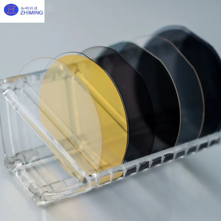
- Verschiedene Kristallschliffe: X-Schliff / Y-Schliff / Z-Schliff
- Wafergrößen: 3 Zoll / 4 Zoll / 6 Zoll / 8 Zoll
Wafer-Struktur
| Ebene | Material | Funktion |
|---|---|---|
| Oberste Ebene | LiNbO₃-Dünnschicht (TFLN) | Elektrooptische und nichtlineare optische Funktionen |
| Mittlere Schicht | SiO₂ (vergrabenes Oxid) | Optische Isolierung und Einschränkung |
| Unterste Schicht | Silizium / Quarz / Saphir | Mechanische Unterstützung und CMOS-Kompatibilität |
Technische Daten
Wafer-Spezifikationen
| Parameter | Wert |
|---|---|
| Waferdurchmesser | 3″, 4″, 6″, 8″ |
| Gesamtdicke | 525 ± 25 μm |
| Bogen | ±50 μm |
| Warp | <50 μm |
| LTV | <1,5 μm (5 × 5 mm², 95%) |
Dünnschicht aus Lithiumniobat
| Parameter | Wert |
|---|---|
| Material | LiNbO₃-Einkristall |
| Dicke | 300 nm – 1000 nm |
| Ausrichtungsgenauigkeit | ±0,5° |
| Oberflächenrauhigkeit | Ra < 1 nm |
| Haftungsfehler | Keine Fehler >1 mm |
Vergrabene Oxidschicht (SiO₂)
| Parameter | Wert |
|---|---|
| Material | SiO₂ |
| Dicke | 100 nm – 2 μm (anpassbar) |
| Einheitlichkeit | ±5% |
 Herstellungsverfahren
LNOI-Wafer werden unter Verwendung von Verfahren in Halbleiterqualität hergestellt:
- Ionenimplantation zur kontrollierten Schichttrennung
- Wafer-Bonding auf isolierende Substrate
- Hochtemperaturglühen zur Kristallstabilisierung
- Chemisch-mechanisches Polieren (CMP) zur Oberflächenplanarisierung
- Abschließende Prüfung der optischen und baulichen Qualität
Wichtigste Anwendungsbereiche
- Optische Hochgeschwindigkeitskommunikation (100G–800G-Modulatoren)
- Quantenphotonik (Erzeugung verschränkter Photonen, QKD-Systeme)
- Mikrowellenphotonik (HF-Signalverarbeitung, Millimeterwellen-Systeme)
- Nichtlineare Optik (Frequenzkonversion, optische Kämme)
- Integrierte Sensorsysteme (biochemische und optische Resonatoren)
Leistungsvorteil gegenüber LiNbO₃ in Großmengen
| Eigentum | LiNbO₃ in Großmengen | LNOI-Dünnschicht |
|---|---|---|
| Optischer Verlust | Höher | <0,05 dB/cm |
| Integration | Niedrig | Hochdichte Photonik |
| Gerätegröße | Groß | Submikrometerbereich |
| CMOS-Kompatibilität | Nein | Ja |
| Modulationseffizienz | Mäßig | Hoch (Vπ ~1 V erreichbar) |
Anpassungsoptionen
| Option | Beschreibung |
|---|---|
| Kristallschliff | X-Schnitt / Y-Schnitt / Z-Schnitt |
| Filmdicke | 300 nm – 1000 nm |
| Substrat | Silizium / Quarz / Saphir |
| Oxidschicht | 100 nm – 2 μm (kundenspezifisch) |
| Doping | MgO-dotiertes LiNbO₃ erhältlich |
Qualitätskontrolle
| Testaufgabe | Methode |
|---|---|
| Optischer Verlust | Ausbreitungstest für Wellenleiter |
| Oberflächenrauhigkeit | AFM-Messung |
| Gleichmäßigkeit der Dicke | Kartensystem |
| Klebequalität | IR-Prüfung |
| Ebenheit | Wafer-Messtechnik |
Technische Kompetenz
ZMSH bietet umfassende Unterstützung für die gesamte LNOI-Wafer-Entwicklung:
- Optimierung des Dünnschichtdesigns
- Verfahrenstechnik beim Wafer-Bonding
- Unterstützung bei der Herstellung photonischer Bauelemente
- Nanofabrikation (EBL / IBE)
- Prüfung und Validierung der optischen Leistung
Unterstützt sowohl die Prototypenentwicklung in der Forschung und Entwicklung als auch die skalierbare Kleinserienfertigung für Wafer bis zu einer Größe von 8 Zoll.
FAQ
Wozu dient LNOI?
LNOI-Wafer finden breite Anwendung in der optischen Kommunikation, der Quantenphotonik, der nichtlinearen Optik und bei integrierten photonischen Schaltungen.
Wie groß ist die typische Dünnschichtdicke?
Die Dicke typischer Lithiumniobat-Dünnschichten liegt zwischen 300 nm und 1000 nm.
Warum sollte man LNOI anstelle von Lithium-Niobat in loser Form verwenden?
LNOI bietet geringere optische Verluste, eine höhere Integrationsdichte und eine CMOS-kompatible photonische Integration.
Lässt sich LNOI in die Siliziumphotonik integrieren?
Ja, LNOI ist vollständig kompatibel mit photonischen Plattformen aus Silizium und Siliziumnitrid.

Rezensionen
Es gibt noch keine Rezensionen.