

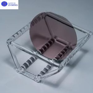
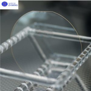
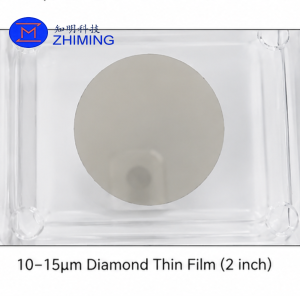
 تُعد رقائق النيوبيت الليثيوم ذات الطبقة الرقيقة على عازل (LNOI) ركائز ضوئية متطورة تُستخدم في الأنظمة الضوئية المتكاملة، والأنظمة الضوئية التي تعمل بالموجات الدقيقة، والأنظمة الكمومية.
يتكون الهيكل من طبقة رقيقة من نيوبيت الليثيوم أحادي البلورة، ملتصقة بطبقة عازلة من ثاني أكسيد السيليكون ومدعومة بركيزة من السيليكون.
يوفر هذا التصميم حصرًا ضوئيًا قويًا، وفقدانًا منخفضًا للغاية في الانتشار، وكفاءة كهروضوئية عالية، مما يجعله منصة أساسية في مجال الضوئيات المتكاملة.
ما هو نيوبيت الليثيوم ذو الطبقة الرقيقة (TFLN)
يشير مصطلح «نيوبات الليثيوم ذو الطبقة الرقيقة» (TFLN) إلى طبقة بلورية من مادة LiNbO₃ يقل سمكها عن الميكرون، وقد صُممت خصيصًا للاستخدام في الدليل الموجي البصري والتطبيقات الكهروضوئية.
بالمقارنة مع نيوبات الليثيوم السائب، يتيح TFLN احتواءً بصريًا أكثر إحكامًا، وحجمًا أصغر للأجهزة، وكثافة تكامل أعلى.
يتم عادةً تنفيذ شبكة LNOI على رقائق LNOI لتشكيل منصة ضوئية متكاملة.
 الميزات الرئيسية
- خسارة بصرية منخفضة للغاية < 0.05 ديسيبل/سم عند 1550 نانومتر
- معامل كهرو-بصري عالٍ (r₃₃ يصل إلى 90 بيكومتر/فولت)
- التوافق مع موجات الدليل الموجي ذات الحجم الأصغر من الميكرون (<1 ميكرومتر)
- تكامل متوافق مع CMOS مع منصات Si / SiN
- استقرار حراري عالٍ (درجة حرارة كوري تبلغ حوالي 1140 درجة مئوية)
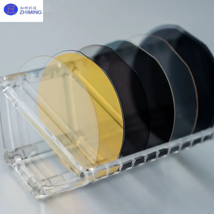
- قطع بلورية متعددة: قطع X / قطع Y / قطع Z
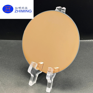
- أحجام الرقائق: 3 بوصات / 4 بوصات / 6 بوصات / 8 بوصات
هيكل الرقاقة
| طبقة | المواد | الوظيفة |
|---|---|---|
| الطبقة العلوية | طبقة رقيقة من LiNbO₃ (TFLN) | الوظائف الكهروضوئية والوظائف البصرية غير الخطية |
| الطبقة الوسطى | SiO₂ (أكسيد مدفون) | العزل البصري والحصر البصري |
| الطبقة السفلية | السيليكون / الكوارتز / الياقوت | الدعم الميكانيكي والتوافق مع CMOS |
المواصفات الفنية
مواصفات الرقاقة
| المعلمة | القيمة |
|---|---|
| قطر الرقاقة | 3 بوصات، 4 بوصات، 6 بوصات، 8 بوصات |
| السماكة الإجمالية | 525 ± 25 ميكرومتر |
| القوس | ±50 ميكرومتر |
| الاعوجاج | أقل من 50 ميكرومتر |
| LTV | أقل من 1.5 ميكرومتر (5×5 مم²، 95%) |
طبقة رقيقة من نيوبات الليثيوم
| المعلمة | القيمة |
|---|---|
| المواد | LiNbO₃ أحادي البلورة |
| السُمك | 300 نانومتر – 1000 نانومتر |
| دقة التوجيه | ±0.5 درجة |
| خشونة السطح | Ra < 1 نانومتر |
| عيوب الترابط | لا توجد عيوب أكبر من 1 مم |
طبقة أكسيد مدفونة (SiO₂)
| المعلمة | القيمة |
|---|---|
| المواد | ثاني أكسيد السيليكون |
| السُمك | 100 نانومتر – 2 ميكرومتر (قابلة للتخصيص) |
| التوحيد | ±5% |
 عملية التصنيع
يتم تصنيع رقائق LNOI باستخدام عمليات خاصة بأشباه الموصلات:
- زرع الأيونات من أجل فصل الطبقات بشكل متحكم فيه
- ربط الرقائق على ركائز عازلة
- التلدين بدرجة حرارة عالية لتثبيت البنية البلورية
- التلميع الكيميائي الميكانيكي (CMP) لتسوية الأسطح
- الفحص النهائي للجودة البصرية والهيكلية
التطبيقات الرئيسية
- الاتصالات الضوئية عالية السرعة (مُعدِّلات 100G–800G)
- الضوئيات الكمومية (توليد الفوتونات المتشابكة، أنظمة التشفير الكمومي)
- ضوئيات الموجات الدقيقة (معالجة إشارات الترددات اللاسلكية، أنظمة الموجات المليمترية)
- البصريات غير الخطية (تحويل التردد، الأمشاط الضوئية)
- أنظمة الاستشعار المتكاملة (مرنانات كيميائية حيوية وبصرية)
مزايا الأداء مقارنة بـ LiNbO₃ السائب
| الممتلكات | LiNbO₃ السائب | LNOI للأغشية الرقيقة |
|---|---|---|
| الخسارة البصرية | أعلى | <0.05 ديسيبل/سم |
| التكامل | منخفضة | الضوئيات عالية الكثافة |
| حجم الجهاز | كبير | مقياس دون الميكرون |
| التوافق مع CMOS | لا | نعم |
| كفاءة التعديل | معتدل | عالية (يمكن الوصول إلى Vπ ~1 فولت) |
خيارات التخصيص
| خيار | الوصف |
|---|---|
| القطع البلوري | قطع على المحور X / قطع على المحور Y / قطع على المحور Z |
| سُمك الفيلم | 300 نانومتر – 1000 نانومتر |
| الركيزة | السيليكون / الكوارتز / الياقوت |
| طبقة الأكسيد | 100 نانومتر – 2 ميكرومتر (حسب الطلب) |
| المنشطات | يتوفر LiNbO₃ المُشبَّع بالمغنيسيوم |
مراقبة الجودة
| عنصر الاختبار | الطريقة |
|---|---|
| الخسارة البصرية | اختبار انتشار الموجة في الدليل الموجي |
| خشونة السطح | قياس AFM |
| توحيد السُمك | نظام رسم الخرائط |
| جودة الترابط | الفحص بالأشعة تحت الحمراء |
| التسطيح | قياس الرقائق |
القدرات الهندسية
ZMSH تقدم الدعم الكامل لجميع مراحل عملية تطوير رقائق LNOI:
- تحسين تصميم الأغشية الرقيقة
- هندسة عمليات ربط الرقائق
- دعم تصنيع الأجهزة الضوئية
- التصنيع النانوي (EBL / IBE)
- اختبار الأداء البصري والتحقق منه
يدعم كلاً من إنشاء النماذج الأولية لأغراض البحث والتطوير والإنتاج القابل للتوسع بكميات صغيرة حتى رقائق بحجم 8 بوصات.
الأسئلة الشائعة
ما هو الغرض من LNOI؟
تُستخدم رقائق LNOI على نطاق واسع في مجال الاتصالات الضوئية، والضوئيات الكمومية، والبصريات غير الخطية، والدوائر الضوئية المتكاملة.
ما هو السُمك النموذجي للطبقة الرقيقة؟
يتراوح سمك الطبقة الرقيقة النموذجية لنيوبيت الليثيوم بين 300 نانومتر و1000 نانومتر.
لماذا يُفضل استخدام LNOI بدلاً من نيوبيت الليثيوم السائب؟
توفر تقنية LNOI خسارة ضوئية أقل، وكثافة تكامل أعلى، وتكامل ضوئي متوافق مع تقنية CMOS.
هل يمكن أن تتكامل تقنية LNOI مع تقنية الضوئيات السليكونية؟
نعم، تتوافق تقنية LNOI تمامًا مع المنصات الضوئية المصنوعة من السيليكون ونيتريد السيليكون.

المراجعات
لا توجد مراجعات بعد.