

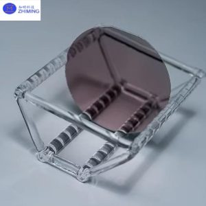
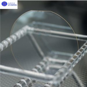
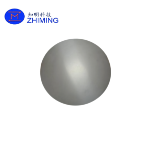
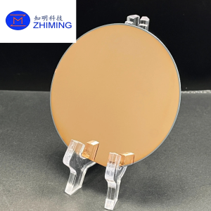
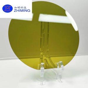
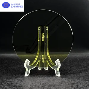
 Тонкопленочные пластины из ниобата лития на изоляторе (LNOI) представляют собой современные фотонные подложки, применяемые в интегрированных оптических, микроволновых фотонных и квантовых системах.
Конструкция состоит из тонкой пленки монокристаллического ниобата лития, нанесенной на изолирующий слой SiO₂ и закрепленной на кремниевой подложке.
Данная конфигурация обеспечивает сильное оптическое локализование, сверхнизкие потери в линии прохождения и высокую электрооптическую эффективность, что делает её ключевой платформой для интегрированной фотоники.
Что такое тонкопленочный ниобат лития (TFLN)
Тонкопленочный ниобат лития (TFLN) представляет собой субмикронный кристаллический слой LiNbO₃, разработанный для использования в оптических волноводах и электрооптических системах.
По сравнению с объемным ниобатом лития, TFLN обеспечивает более плотное оптическое локализование, меньшие габариты устройства и более высокую плотность интеграции.
TFLN обычно реализуется на подложках LNOI для создания полноценной интегрированной фотонной платформы.
 Основные характеристики
- Сверхнизкие оптические потери < 0,05 дБ/см при длине волны 1550 нм
- Высокий электрооптический коэффициент (r₃₃ до 90 пм/В)
- Совместимость с волноводами субмикронного размера (<1 мкм)
- Интеграция, совместимая с CMOS, с платформами Si / SiN
- Высокая термическая стабильность (температура Кюри ~1140 °C)
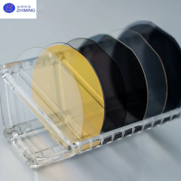
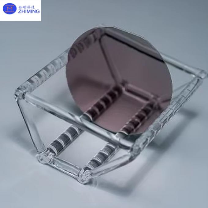
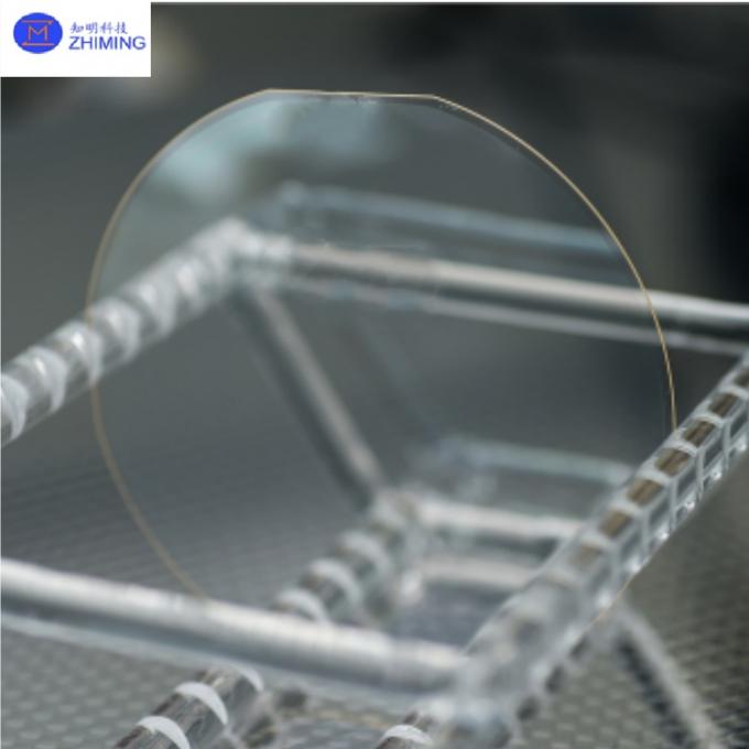
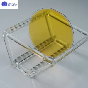
- Различные типы огранки: X-огранка / Y-огранка / Z-огранка
- Размеры пластин: 3 дюйма / 4 дюйма / 6 дюймов / 8 дюймов
Структура пластины
| Слой | Материал | Функция |
|---|---|---|
| Верхний слой | Тонкая пленка LiNbO₃ (TFLN) | Электрооптические и нелинейные оптические функции |
| Средний слой | SiO₂ (покрытый оксид) | Оптическая изоляция и локализация |
| Нижний слой | Кремний / Кварц / Сапфир | Механическая поддержка и совместимость с CMOS |
Технические характеристики
Технические характеристики пластин
| Параметр | Значение |
|---|---|
| Диаметр пластины | 3 дюйма, 4 дюйма, 6 дюймов, 8 дюймов |
| Общая толщина | 525 ± 25 мкм |
| Лук | ±50 мкм |
| Warp | <50 мкм |
| LTV | <1,5 мкм (5×5 мм², 95%) |
Тонкопленочный слой ниобата лития
| Параметр | Значение |
|---|---|
| Материал | Монокристаллический LiNbO₃ |
| Толщина | 300 нм – 1000 нм |
| Точность ориентации | ±0,5° |
| Шероховатость поверхности | Ra < 1 нм |
| Дефекты сцепления | Отсутствие дефектов размером более 1 мм |
Слой погруженного оксида (SiO₂)
| Параметр | Значение |
|---|---|
| Материал | SiO₂ |
| Толщина | 100 нм – 2 мкм (настраиваемый диапазон) |
| Равномерность | ±5% |
 Технология изготовления
Пластины LNOI изготавливаются с использованием технологий полупроводникового производства:
- Ионная имплантация для контролируемого разделения слоев
- Склеивание пластин с изолирующими подложками
- Высокотемпературный отжиг для стабилизации кристаллов
- Химико-механическая полировка (CMP) для выравнивания поверхности
- Заключительный контроль качества оптических и конструктивных характеристик
Основные области применения
- Высокоскоростная оптическая связь (модуляторы 100G–800G)
- Квантовая фотоника (генерация запутанных фотонов, системы квантовой криптографии)
- Микроволновый фотоника (обработка радиочастотных сигналов, системы миллиметрового диапазона)
- Нелинейная оптика (преобразование частоты, оптические гребни)
- Интегрированные сенсорные системы (биохимические и оптические резонаторы)
Преимущества по характеристикам по сравнению с LiNbO₃ в массовом исполнении
| Недвижимость | LiNbO₃ в рассыпном виде | Тонкопленочная LNOI |
|---|---|---|
| Оптические потери | Выше | <0,05 дБ/см |
| Интеграция | Низкий | Фотоника высокой плотности |
| Размер устройства | Большой | Субмикронный масштаб |
| Совместимость с CMOS | Нет | Да |
| Коэффициент модуляции | Умеренный | Высокий (возможно достичь Vπ ~1 В) |
Параметры настройки
| Вариант | Описание |
|---|---|
| Кристальная огранка | X-образный разрез / Y-образный разрез / Z-образный разрез |
| Толщина пленки | 300 нм – 1000 нм |
| Подложка | Кремний / Кварц / Сапфир |
| Оксидный слой | 100 нм – 2 мкм (по заказу) |
| Допинг | В наличии LiNbO₃, легированный MgO |
Контроль качества
| Тестовый вопрос | Метод |
|---|---|
| Оптические потери | Испытание распространения в волноводе |
| Шероховатость поверхности | Атомно-силовая микроскопия |
| Равномерность толщины | Система картографирования |
| Качество склеивания | Инфракрасный контроль |
| Плоскость | Метрология пластин |
Инженерный потенциал
ZMSH обеспечивает комплексную поддержку на всех этапах разработки пластин LNOI:
- Оптимизация конструкции тонкопленочных устройств
- Технология склеивания пластин
- Поддержка в изготовлении фотонных устройств
- Нанотехнологии (EBL / IBE)
- Тестирование и проверка оптических характеристик
Поддерживает как создание прототипов в рамках НИОКР, так и масштабируемое мелкосерийное производство с использованием пластин размером до 8 дюймов.
ЧАСТО ЗАДАВАЕМЫЕ ВОПРОСЫ
Для чего используется LNOI
Пластины LNOI широко используются в оптической связи, квантовой фотонике, нелинейной оптике и интегральных фотонных схемах.
Какова типичная толщина тонкой пленки?
Толщина типичной тонкой пленки ниобата лития колеблется от 300 до 1000 нм.
Почему стоит использовать LNOI вместо ниобата лития в массовом производстве
Технология LNOI обеспечивает меньшие оптические потери, более высокую плотность интеграции и возможность интеграции с CMOS-схемами.
Может ли LNOI интегрироваться с кремниевой фотоникой?
Да, LNOI полностью совместима с фотонными платформами на основе кремния и нитрида кремния.
Отзывы
Отзывов пока нет.