

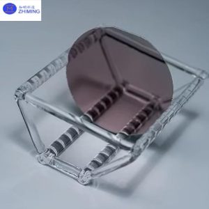
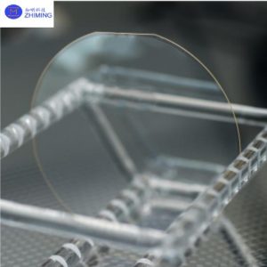
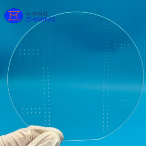
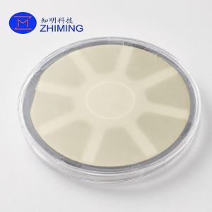
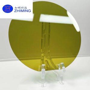
 แผ่นเวเฟอร์ Thin-Film Lithium Niobate on Insulator (LNOI) เป็นวัสดุพื้นฐานโฟโทนิกขั้นสูงที่ใช้สำหรับระบบออปติคัลแบบบูรณาการ ระบบโฟโทนิกไมโครเวฟ และระบบควอนตัม.
โครงสร้างประกอบด้วยฟิล์มบางของลิเทียมไนโอเบตผลึกเดี่ยวที่เชื่อมต่อกับชั้นฉนวน SiO₂ และรองรับด้วยแผ่นซิลิคอน.
การกำหนดค่านี้ให้การกักเก็บแสงที่แข็งแกร่ง การสูญเสียการแพร่กระจายต่ำมาก และประสิทธิภาพทางอิเล็กโทร-ออปติกสูง ทำให้เป็นแพลตฟอร์มสำคัญสำหรับโฟโตนิกส์แบบบูรณาการ.
ฟิล์มบางลิเธียมไนโอเบต (TFLN) คืออะไร
ฟิล์มบางลิเทียมไนโอเบต (TFLN) หมายถึงชั้นผลึก LiNbO₃ ที่มีขนาดต่ำกว่าไมโครเมตร ซึ่งถูกออกแบบทางวิศวกรรมสำหรับใช้งานในอุปกรณ์นำคลื่นแสงและอุปกรณ์อิเล็กโทรออปติก.
เมื่อเปรียบเทียบกับลิเธียมไนโอเบตแบบมวลรวม TFLN ช่วยให้สามารถกักเก็บแสงได้แน่นกว่า มีขนาดอุปกรณ์ที่เล็กลง และมีความหนาแน่นในการรวมระบบที่สูงกว่า.
TFLN มักจะถูกนำไปใช้บนเวเฟอร์ LNOI เพื่อสร้างแพลตฟอร์มโฟโตนิกแบบบูรณาการอย่างสมบูรณ์.
 คุณสมบัติเด่น
- การสูญเสียทางแสงต่ำเป็นพิเศษ < 0.05 dB/cm @ 1550 นาโนเมตร
- ค่าสัมประสิทธิ์อิเล็กโทร-ออปติกสูง (r₃₃ สูงถึง 90 pm/V)
- ความเข้ากันได้ของคลื่นนำทางขนาดต่ำกว่าไมครอน (<1 ไมโครเมตร)
- การรวมที่เข้ากันได้กับ CMOS กับแพลตฟอร์ม Si / SiN
- ความเสถียรทางความร้อนสูง (~1140°C อุณหภูมิเคอรี)
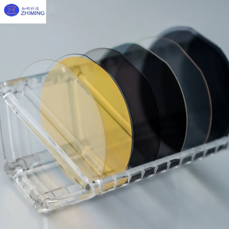
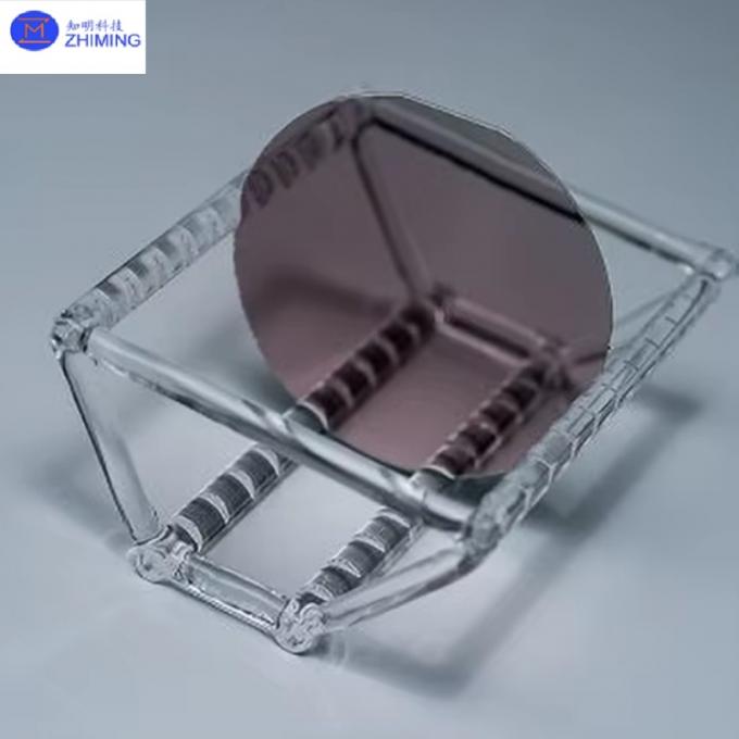
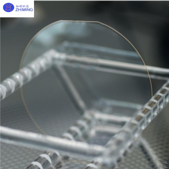
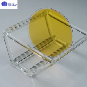
- การเจียระไนคริสตัลหลายแบบ: เจียระไนแบบ X / เจียระไนแบบ Y / เจียระไนแบบ Z
- ขนาดเวเฟอร์: 3 นิ้ว / 4 นิ้ว / 6 นิ้ว / 8 นิ้ว
โครงสร้างเวเฟอร์
| ชั้น | วัสดุ | ฟังก์ชัน |
|---|---|---|
| ชั้นบนสุด | ฟิล์มบาง LiNbO₃ (TFLN) | ฟังก์ชันการทำงานทางไฟฟ้า-แสงและแสงไม่เชิงเส้น |
| ชั้นกลาง | SiO₂ (ออกไซด์ฝังตัว) | การแยกและกักเก็บด้วยแสง |
| ชั้นล่างสุด | ซิลิกอนไดออกไซด์ / ควอตซ์ / แซฟไฟร์ | การสนับสนุนทางกลไกและความเข้ากันได้กับ CMOS |
ข้อมูลจำเพาะทางเทคนิค
ข้อมูลจำเพาะของเวเฟอร์
| พารามิเตอร์ | มูลค่า |
|---|---|
| เส้นผ่านศูนย์กลางของเวเฟอร์ | 3 นิ้ว, 4 นิ้ว, 6 นิ้ว, 8 นิ้ว |
| ความหนาทั้งหมด | 525 ± 25 ไมโครเมตร |
| โบว์ | ±50 ไมโครเมตร |
| วาร์ป | <50 ไมโครเมตร |
| LTV | <1.5 μm (5×5 มม.², 95%) |
ชั้นฟิล์มบางลิเธียมไนโอเบต
| พารามิเตอร์ | มูลค่า |
|---|---|
| วัสดุ | ผลึกเดี่ยว LiNbO₃ |
| ความหนา | 300 นาโนเมตร – 1000 นาโนเมตร |
| ความถูกต้องของการวัดทิศทาง | ±0.5° |
| ความหยาบผิว | Ra < 1 นาโนเมตร |
| ข้อบกพร่องในการยึดติด | ไม่มีตำหนิ >1 มม. |
ชั้นออกไซด์ฝังตัว (SiO₂)
| พารามิเตอร์ | มูลค่า |
|---|---|
| วัสดุ | ซิลิกอนไดออกไซด์ |
| ความหนา | 100 นาโนเมตร – 2 ไมโครเมตร (ปรับแต่งได้) |
| ความสม่ำเสมอ | ±5% |
 กระบวนการผลิต
เวเฟอร์ LNOI ผลิตขึ้นโดยใช้กระบวนการระดับเซมิคอนดักเตอร์:
- การฝังไอออนเพื่อการแยกชั้นที่ควบคุมได้
- การยึดเกาะเวเฟอร์ลงบนวัสดุฉนวน
- การอบชุบด้วยความร้อนสูงเพื่อความเสถียรของผลึก
- การขัดผิวด้วยเคมีเชิงกล (CMP) สำหรับการปรับผิวให้เรียบ
- การตรวจสอบคุณภาพทางแสงและโครงสร้างขั้นสุดท้าย
การใช้งานหลัก
- การสื่อสารด้วยแสงความเร็วสูง (ตัวมอดูเลต 100G–800G)
- โฟโตนิกส์ควอนตัม (การสร้างโฟตอนที่พันกัน, ระบบ QKD)
- โฟโตนิกส์ไมโครเวฟ (การประมวลผลสัญญาณ RF, ระบบ mmWave)
- ออปติกส์แบบไม่เชิงเส้น (การแปลงความถี่, หวีแสง)
- ระบบตรวจวัดแบบบูรณาการ (ตัวกักเก็บเชิงชีวเคมีและเชิงแสง)
ข้อได้เปรียบด้านประสิทธิภาพเมื่อเทียบกับ LiNbO₃ แบบจำนวนมาก
| ทรัพย์สิน | LiNbO₃ จำนวนมาก | ฟิล์มบาง LNOI |
|---|---|---|
| การสูญเสียทางแสง | สูงขึ้น | น้อยกว่า 0.05 เดซิเบลต่อเซนติเมตร |
| การบูรณาการ | ต่ำ | โฟโตนิกส์ความหนาแน่นสูง |
| ขนาดของอุปกรณ์ | ใหญ่ | ระดับไมครอน |
| ความเข้ากันได้กับ CMOS | ไม่ | ใช่ |
| ประสิทธิภาพการมอดูเลต | ปานกลาง | สูง (Vπ ~1V สามารถทำได้) |
ตัวเลือกการปรับแต่ง
| ตัวเลือก | คำอธิบาย |
|---|---|
| คริสตัลคัท | เอ็กซ์คัท / วายคัท / ซีคัท |
| ความหนาของฟิล์ม | 300 นาโนเมตร – 1000 นาโนเมตร |
| วัสดุรองรับ | ซิลิกอนไดออกไซด์ / ควอตซ์ / แซฟไฟร์ |
| ชั้นออกไซด์ | 100 นาโนเมตร – 2 ไมโครเมตร (สั่งทำพิเศษ) |
| การใช้สารกระตุ้น | มี MgO-doped LiNbO₃ ให้บริการ |
การควบคุมคุณภาพ
| รายการทดสอบ | วิธีการ |
|---|---|
| การสูญเสียทางแสง | การทดสอบการแพร่กระจายของคลื่นนำคลื่น |
| ความหยาบผิว | การวัดด้วยกล้องจุลทรรศน์แบบแรงอะตอม |
| ความสม่ำเสมอของความหนา | ระบบแผนที่ |
| คุณภาพการเชื่อมติด | การตรวจสอบด้วยอินฟราเรด |
| ความเรียบ | การวัดขนาดเวเฟอร์ |
ความสามารถทางวิศวกรรม
ZMSH ให้การสนับสนุนกระบวนการทั้งหมดสำหรับการพัฒนาเวเฟอร์ LNOI:
- การเพิ่มประสิทธิภาพการออกแบบฟิล์มบาง
- วิศวกรรมกระบวนการยึดเกาะเวเฟอร์
- การสนับสนุนการผลิตอุปกรณ์โฟโตนิก
- นาโนฟราบิเคชั่น (EBL / IBE)
- การทดสอบและตรวจสอบความถูกต้องของประสิทธิภาพทางแสง
รองรับทั้งการสร้างต้นแบบสำหรับการวิจัยและพัฒนา และการผลิตแบบเป็นชุดขนาดเล็กที่สามารถขยายได้ถึงแผ่นเวเฟอร์ขนาด 8 นิ้ว.
คำถามที่พบบ่อย
LNOI ใช้สำหรับอะไร
แผ่นเวเฟอร์ LNOI ถูกใช้อย่างแพร่หลายในด้านการสื่อสารทางแสง, ควอนตัมโฟโตนิกส์, ออปติกส์เชิงไม่เชิงเส้น, และวงจรโฟโตนิกส์แบบบูรณาการ.
ความหนาของฟิล์มบางโดยทั่วไปคืออะไร
ความหนาของฟิล์มบางลิเธียมไนโอเบตทั่วไปอยู่ระหว่าง 300 นาโนเมตร ถึง 1,000 นาโนเมตร.
ทำไมต้องใช้ LNOI แทนลิเธียมไนโอเบตแบบมวล
LNOI ให้การสูญเสียทางแสงที่ต่ำกว่า ความหนาแน่นในการรวมที่สูงกว่า และการรวมโฟตอนที่เข้ากันได้กับ CMOS.
LNOI สามารถผสานรวมกับซิลิคอนโฟโตนิกส์ได้หรือไม่
ใช่, LNOI สามารถใช้งานร่วมกับแพลตฟอร์มโฟโตนิกซิลิคอนและซิลิคอนไนไตรด์ได้อย่างสมบูรณ์.

รีวิว
ยังไม่มีบทวิจารณ์