

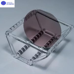
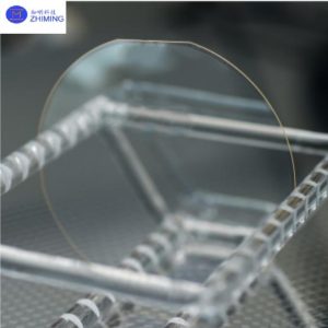
 절연체 상의 박막 니오베이트 리튬(LNOI) 웨이퍼는 집적 광학, 마이크로파 광학 및 양자 시스템에 사용되는 첨단 광학 기판입니다.
이 구조는 SiO₂ 절연층 위에 접합되고 실리콘 기판에 지지된 단결정 니오베이트 리튬 박막으로 구성되어 있다.
이 구성은 강력한 광학 국소화, 초저 전파 손실, 높은 전기-광학 효율을 제공하여 집적 광학 분야의 핵심 플랫폼으로 자리매김하고 있습니다.
박막 리튬 니오베이트(TFLN)란 무엇인가
박막 니오베이트 리튬(TFLN)은 광 도파로 및 전기광학 응용을 위해 설계된 서브미크론 크기의 결정질 LiNbO₃ 층을 의미합니다.
대량 리튬 니오베이트와 비교할 때, TFLN은 더 정밀한 광학 국소화, 더 작은 소자 크기와 더 높은 집적 밀도를 가능하게 합니다.
TFLN은 일반적으로 LNOI 웨이퍼에 구현되어 완전한 통합 광학 플랫폼을 구성합니다.
 주요 기능
주요 기능
- 초저 광 손실 < 0.05 dB/cm (1550 nm)
- 높은 전기광학 계수 (r₃₃ 최대 90 pm/V)
- 서브마이크론 파장 가이드 호환성 (<1 μm)
- Si/SiN 플랫폼과의 CMOS 호환 통합
- 높은 열적 안정성 (퀴리 온도 약 1140°C)
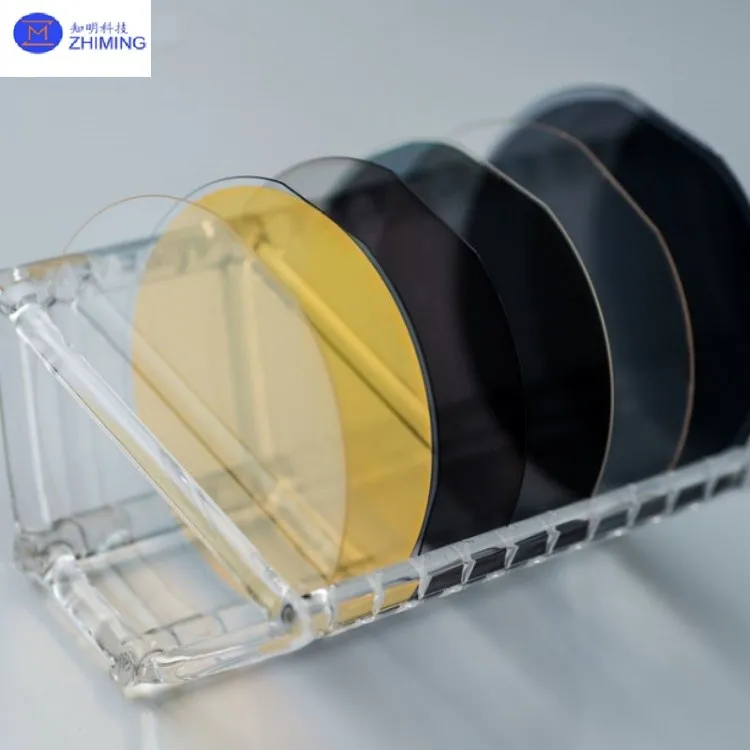
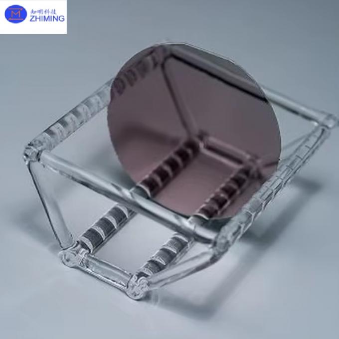
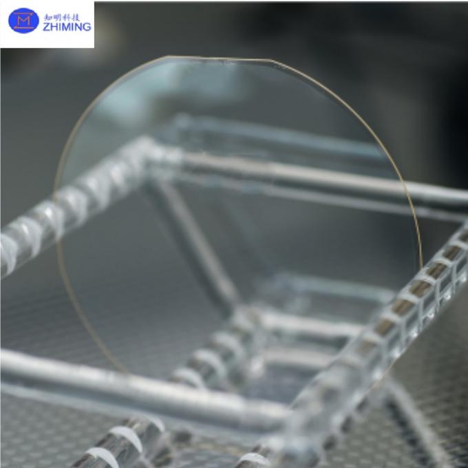
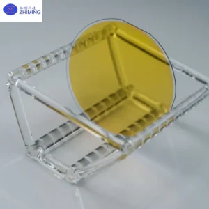
- 다양한 크리스탈 커팅 방식: X-컷 / Y-컷 / Z-컷
- 웨이퍼 크기: 3인치 / 4인치 / 6인치 / 8인치
웨이퍼 구조
| 레이어 | 재료 | 기능 |
|---|---|---|
| 상단 레이어 | LiNbO₃ 박막 (TFLN) | 전기광학 및 비선형 광학 기능 |
| 중간층 | SiO₂ (매립 산화막) | 광학적 격리 및 국한 |
| 바닥층 | 실리콘 / 석영 / 사파이어 | 기계적 지원 및 CMOS 호환성 |
기술 사양
웨이퍼 사양
| 매개변수 | 가치 |
|---|---|
| 웨이퍼 직경 | 3인치, 4인치, 6인치, 8인치 |
| 총 두께 | 525 ± 25 μm |
| 활 | ±50 μm |
| 워프 | 50 μm 미만 |
| LTV | <1.5 μm (5×5 mm², 95%) |
박막 니오베이트 리튬 층
| 매개변수 | 가치 |
|---|---|
| 재료 | 단결정 LiNbO₃ |
| 두께 | 300 nm – 1000 nm |
| 방향 정확도 | ±0.5° |
| 표면 거칠기 | Ra < 1 nm |
| 접합 결함 | 1mm를 초과하는 결함 없음 |
매립 산화막 (SiO₂)
| 매개변수 | 가치 |
|---|---|
| 재료 | 이산화규소 |
| 두께 | 100 nm – 2 μm (맞춤 설정 가능) |
| 균일성 | ±5% |
 제조 공정
제조 공정
LNOI 웨이퍼는 반도체 등급 공정을 통해 제조됩니다:
- 제어된 층 분리를 위한 이온 주입
- 절연 기판에 대한 웨이퍼 본딩
- 결정 안정화를 위한 고온 어닐링
- 표면 평탄화를 위한 화학적 기계적 연마(CMP)
- 최종 광학 및 구조적 품질 검사
주요 용도
- 고속 광통신 (100G–800G 변조기)
- 양자 광학 (얽힌 광자 생성, QKD 시스템)
- 마이크로파 광학 (RF 신호 처리, 밀리미터파 시스템)
- 비선형 광학 (주파수 변환, 광 빗)
- 통합 감지 시스템 (생화학적 및 광학 공진기)
성능상의 이점 vs 대량 LiNbO₃
| 속성 | 대량 LiNbO₃ | LNOI 박막 |
|---|---|---|
| 광 손실 | 더 높은 | <0.05 dB/cm |
| 통합 | 낮음 | 고밀도 광학 |
| 기기 크기 | 대형 | 서브마이크론 단위 |
| CMOS 호환성 | 아니요 | 네 |
| 변조 효율 | 보통 | 높음 (Vπ 약 1V 달성 가능) |
사용자 지정 옵션
| 옵션 | 설명 |
|---|---|
| 크리스탈 컷 | X-컷 / Y-컷 / Z-컷 |
| 필름 두께 | 300 nm – 1000 nm |
| 기판 | 실리콘 / 석영 / 사파이어 |
| 산화막 | 100 nm – 2 μm (주문 제작) |
| 도핑 | MgO 도핑 LiNbO₃ 공급 가능 |
품질 관리
| 테스트 항목 | 방법 |
|---|---|
| 광 손실 | 도파관 전파 시험 |
| 표면 거칠기 | AFM 측정 |
| 두께 균일성 | 지도 시스템 |
| 접착 품질 | 적외선 검사 |
| 평탄도 | 웨이퍼 계측 |
엔지니어링 역량
ZMSH LNOI 웨이퍼 개발에 대한 전 과정 지원을 제공합니다:
- 박막 설계 최적화
- 웨이퍼 본딩 공정 공학
- 광학 소자 제작 지원
- 나노소자 제조 (EBL / IBE)
- 광학 성능 테스트 및 검증
R&D용 시제품 제작은 물론, 최대 8인치 웨이퍼 규모의 소량 양산까지 지원합니다.
자주 묻는 질문
LNOI는 무엇에 사용되나요?
LNOI 웨이퍼는 광통신, 양자 광학, 비선형 광학 및 집적 광학 회로 분야에서 널리 사용됩니다.
일반적인 박막의 두께는 얼마입니까?
일반적인 니오븀 리튬 박막의 두께는 300 nm에서 1000 nm 사이입니다.
왜 대량 리튬 니오베이트 대신 LNOI를 사용해야 할까요?
LNOI는 낮은 광 손실, 높은 집적 밀도, 그리고 CMOS 호환 광 집적 기술을 제공합니다.
LNOI는 실리콘 포토닉스와 통합될 수 있습니까?
네, LNOI는 실리콘 및 실리콘 질화물 광학 플랫폼과 완벽하게 호환됩니다.
상품평
아직 상품평이 없습니다.