

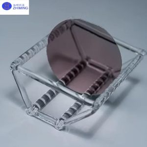
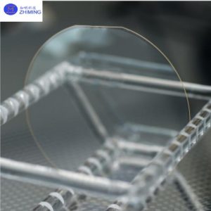
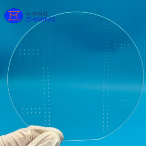
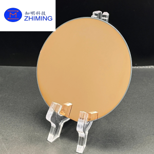
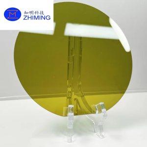
 Các tấm wafer LNOI (Lithium Niobate trên chất cách điện) là các chất nền quang tử tiên tiến được sử dụng trong các hệ thống quang học tích hợp, quang tử vi sóng và hệ thống lượng tử.
Cấu trúc này bao gồm một lớp màng mỏng niobat lithium đơn tinh thể được gắn lên một lớp cách điện SiO₂ và được đặt trên một đế silicon.
Cấu hình này mang lại khả năng giam giữ quang học mạnh mẽ, tổn thất truyền dẫn cực thấp và hiệu suất điện-quang cao, khiến nó trở thành nền tảng quan trọng cho công nghệ quang tử tích hợp.
Lithium Niobate màng mỏng (TFLN) là gì?
Lithium Niobate màng mỏng (TFLN) là một lớp tinh thể LiNbO₃ có độ dày dưới micromet, được thiết kế dành cho các ứng dụng dẫn sóng quang học và điện quang.
So với niobat liti dạng khối, TFLN cho phép giới hạn quang học chặt chẽ hơn, kích thước thiết bị nhỏ gọn hơn và mật độ tích hợp cao hơn.
TFLN thường được triển khai trên các tấm wafer LNOI để tạo thành một nền tảng quang tử tích hợp hoàn chỉnh.
 Các tính năng chính
- Mất mát quang học cực thấp < 0,05 dB/cm ở bước sóng 1550 nm
- Hệ số điện quang cao (r₃₃ lên đến 90 pm/V)
- Khả năng tương thích với ống dẫn sóng có kích thước dưới micromet (<1 μm)
- Tích hợp tương thích CMOS với các nền tảng Si / SiN
- Độ ổn định nhiệt cao (nhiệt độ Curie khoảng 1140°C)
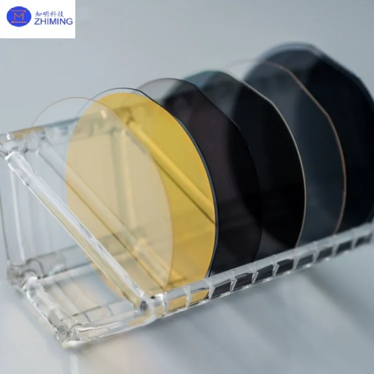
- Nhiều kiểu cắt tinh thể: Cắt X / Cắt Y / Cắt Z
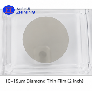
- Kích thước tấm wafer: 3 inch / 4 inch / 6 inch / 8 inch
Cấu trúc tấm wafer
| Lớp | Chất liệu | Chức năng |
|---|---|---|
| Lớp trên cùng | Màng mỏng LiNbO₃ (TFLN) | Chức năng quang điện và quang học phi tuyến |
| Lớp giữa | SiO₂ (Lớp oxit chôn ngầm) | Cách ly và giới hạn quang học |
| Lớp dưới cùng | Silic / Thạch anh / Sapphire | Hỗ trợ cơ học & Tương thích CMOS |
Thông số kỹ thuật
Thông số kỹ thuật của tấm wafer
| Tham số | Giá trị |
|---|---|
| Đường kính tấm wafer | 3″, 4″, 6″, 8″ |
| Tổng độ dày | 525 ± 25 μm |
| Cung | ±50 μm |
| Warp | <50 μm |
| Tỷ lệ cho vay trên giá trị tài sản (LTV) | <1,5 μm (5×5 mm², 95%) |
Lớp màng mỏng niobat liti
| Tham số | Giá trị |
|---|---|
| Chất liệu | LiNbO₃ đơn tinh thể |
| Độ dày | 300 nm – 1000 nm |
| Độ chính xác định hướng | ±0,5° |
| Độ nhám bề mặt | Ra < 1 nm |
| Các khuyết tật liên kết | Không có khuyết tật nào lớn hơn 1 mm |
Lớp oxit chôn ngầm (SiO₂)
| Tham số | Giá trị |
|---|---|
| Chất liệu | SiO₂ |
| Độ dày | 100 nm – 2 μm (có thể tùy chỉnh) |
| Tính đồng nhất | ±5% |
 Quy trình sản xuất
Các tấm wafer LNOI được sản xuất bằng các quy trình đạt tiêu chuẩn bán dẫn:
- Cấy ion để tách lớp có kiểm soát
- Gắn wafer lên các chất nền cách điện
- Quá trình ủ nhiệt độ cao để ổn định tinh thể
- Đánh bóng cơ học hóa học (CMP) để làm phẳng bề mặt
- Kiểm tra chất lượng quang học và cấu trúc lần cuối
Các ứng dụng chính
- Truyền thông quang tốc độ cao (bộ điều chế 100G–800G)
- Quang tử lượng tử (tạo ra photon đan xen, hệ thống QKD)
- Quang tử vi sóng (xử lý tín hiệu tần số vô tuyến, hệ thống sóng milimet)
- Quang học phi tuyến (chuyển đổi tần số, lược quang)
- Hệ thống cảm biến tích hợp (các bộ cộng hưởng sinh hóa và quang học)
Lợi thế về hiệu suất so với LiNbO₃ dạng khối
| Bất động sản | LiNbO₃ dạng khối | LNOI Màng mỏng |
|---|---|---|
| Mất mát quang học | Cao hơn | <0,05 dB/cm |
| Tích hợp | Thấp | Quang tử học mật độ cao |
| Kích thước thiết bị | Lớn | Cấp độ dưới micromet |
| Khả năng tương thích với CMOS | Không | Đúng |
| Hiệu suất điều chế | Trung bình | Cao (có thể đạt được Vπ ~1V) |
Các tùy chọn tùy chỉnh
| Tùy chọn | Mô tả |
|---|---|
| Cắt pha lê | Cắt theo trục X / Cắt theo trục Y / Cắt theo trục Z |
| Độ dày màng | 300 nm – 1000 nm |
| Chất nền | Silic / Thạch anh / Sapphire |
| Lớp oxit | 100 nm – 2 μm (theo yêu cầu) |
| Doping | Có sẵn LiNbO₃ được pha tạp MgO |
Kiểm soát chất lượng
| Câu hỏi trắc nghiệm | Phương pháp |
|---|---|
| Mất mát quang học | Thử nghiệm truyền sóng trong ống dẫn sóng |
| Độ nhám bề mặt | Đo bằng kính hiển vi lực nguyên tử (AFM) |
| Độ đồng đều về độ dày | Hệ thống bản đồ |
| Chất lượng liên kết | Kiểm tra hồng ngoại |
| Độ phẳng | Đo lường tấm wafer |
Năng lực kỹ thuật
ZMSH cung cấp hỗ trợ toàn diện cho quá trình phát triển tấm wafer LNOI:
- Tối ưu hóa thiết kế màng mỏng
- Kỹ thuật quy trình hàn wafer
- Hỗ trợ sản xuất thiết bị quang tử
- Chế tạo nano (EBL / IBE)
- Kiểm tra và xác nhận hiệu suất quang học
Hỗ trợ cả việc chế tạo mẫu thử nghiệm trong nghiên cứu và phát triển (R&D) lẫn sản xuất theo lô nhỏ có thể mở rộng quy mô, lên đến tấm wafer 8 inch.
Câu hỏi thường gặp
LNOI được sử dụng để làm gì?
Các tấm wafer LNOI được sử dụng rộng rãi trong lĩnh vực truyền thông quang học, quang tử lượng tử, quang học phi tuyến và mạch quang tử tích hợp.
Độ dày điển hình của màng mỏng là bao nhiêu?
Độ dày điển hình của màng mỏng niobat liti dao động từ 300 nm đến 1000 nm.
Tại sao nên sử dụng LNOI thay vì niobat lithium dạng khối?
LNOI mang lại mức tổn thất quang học thấp hơn, mật độ tích hợp cao hơn và khả năng tích hợp quang học tương thích với CMOS.
LNOI có thể tích hợp với công nghệ quang tử silicon không?
Đúng vậy, LNOI hoàn toàn tương thích với các nền tảng quang tử silicon và nitrua silicon.
Đánh giá
Chưa có đánh giá nào.