

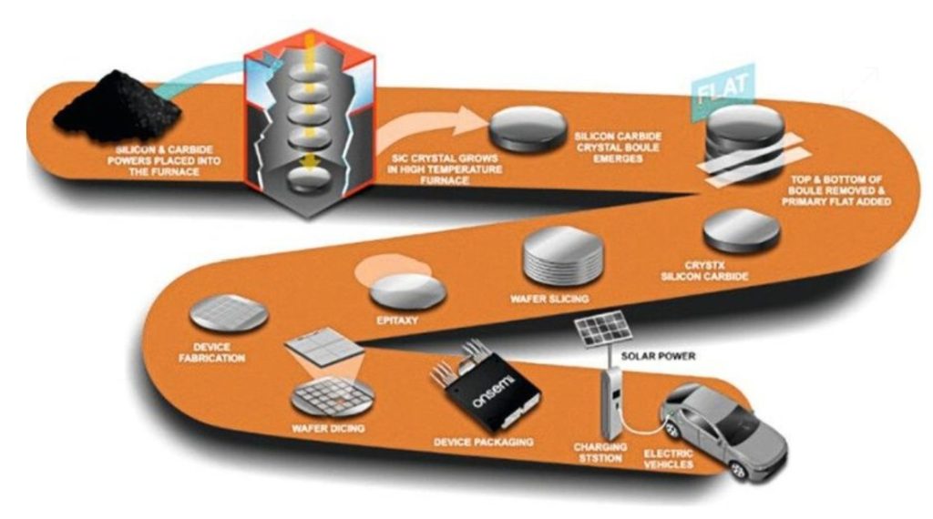
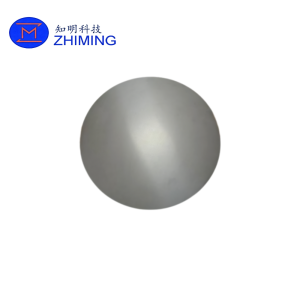
 Tấm wafer epitaxy SiC loại N 6H kích thước 6 inch là một chất nền bán dẫn hiệu suất cao được thiết kế cho các ứng dụng tiên tiến, bao gồm các thiết bị MEMS, cảm biến tia cực tím (UV) và quá trình phát triển graphene epitaxy. Được sản xuất từ các tinh thể đơn tinh thể silicon carbide (SiC) chất lượng cao, tấm wafer này kết hợp các tính chất điện, nhiệt và cơ học xuất sắc, khiến nó trở thành lựa chọn lý tưởng cho các môi trường khắc nghiệt mà các vật liệu silicon thông thường không thể hoạt động đáng tin cậy.
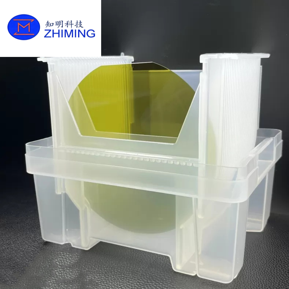
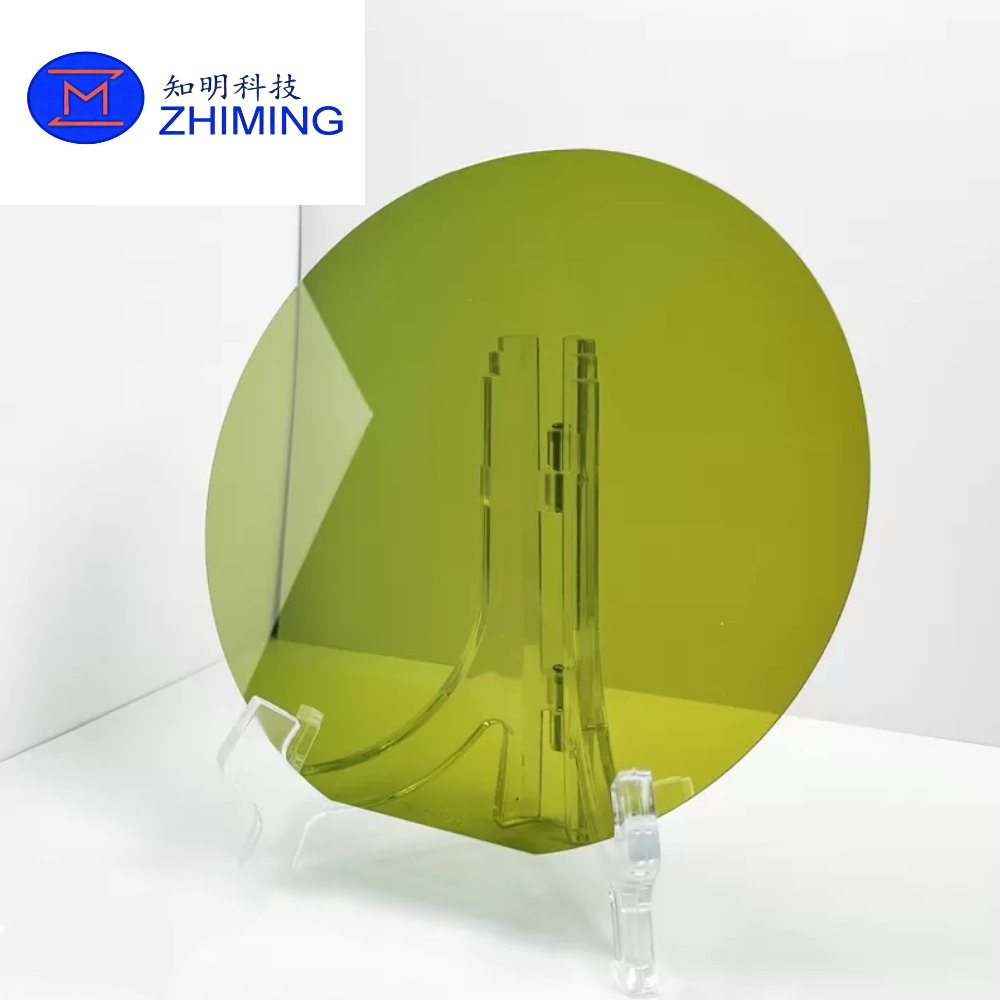
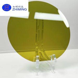
Với đường kính tiêu chuẩn 150 mm (6 inch) và độ dày được kiểm soát chính xác ở mức 350 µm, tấm wafer này mang lại độ ổn định cơ học vượt trội và khả năng tương thích cao với các thiết bị sản xuất bán dẫn hiện đại. Loại tinh thể 6H có khoảng cách năng lượng rộng khoảng 2,96 eV, cho phép hoạt động hiệu quả trong các điều kiện nhiệt độ cao, bức xạ mạnh và môi trường hóa học khắc nghiệt.
Mỗi tấm wafer được xử lý để tạo ra bề mặt sẵn sàng cho quá trình epitaxy bằng công nghệ Đánh bóng Hóa học-Cơ học (CMP) tiên tiến. Điều này đảm bảo độ nhám bề mặt cực thấp, hạn chế tối đa tổn thương bên dưới bề mặt và tạo điều kiện tối ưu cho các quy trình phát triển lớp epitaxy như Phủ hóa học từ hơi (CVD). Kết quả là hiệu suất thiết bị được cải thiện, năng suất cao hơn và độ tin cậy được nâng cao cho các ứng dụng quan trọng.
 Các tính năng chính
Bề mặt sẵn sàng cho quá trình epitaxy nhằm đạt được sự phát triển chất lượng cao
Tấm wafer được cung cấp với bề mặt được đánh bóng bằng phương pháp CMP sáng bóng như gương, đạt độ nhám dưới mức nanomet. Điều này đảm bảo khả năng tương thích tuyệt vời với các quy trình phát triển lớp phủ, đặc biệt là trong quá trình hình thành graphene và sản xuất các thiết bị nhạy cảm với tia UV.
Được tối ưu hóa cho các thiết bị MEMS và môi trường khắc nghiệt
Tấm wafer epitaxy SiC loại N 6H kích thước 6 inch thể hiện độ ổn định nhiệt vượt trội, duy trì hiệu suất hoạt động ở nhiệt độ vượt quá 500°C. Nhờ độ bền cơ học cao và tính trơ hóa học, sản phẩm này rất phù hợp cho các thiết bị MEMS hoạt động trong các môi trường khắc nghiệt như hàng không vũ trụ, năng lượng và hệ thống giám sát công nghiệp.
Khoảng cách dải năng lượng rộng cho các ứng dụng cảm biến tia cực tím
Với khoảng cách dải cấm khoảng 2,96 eV, tấm wafer này có độ nhạy tự nhiên với ánh sáng cực tím nhưng lại không nhạy cảm với các bước sóng trong vùng ánh sáng nhìn thấy. Điều này khiến nó trở thành vật liệu lý tưởng cho các cảm biến tia cực tím không nhạy cảm với ánh sáng mặt trời, được ứng dụng trong phát hiện ngọn lửa, giám sát môi trường và các hệ thống quốc phòng.
Hiệu suất điện ổn định
Việc pha tạp nitơ đảm bảo tính dẫn điện loại N đáng tin cậy, giúp duy trì các đặc tính điện ổn định và hình thành tiếp xúc ohmic bền vững. Điều này là yếu tố thiết yếu đối với các thiết bị cảm biến chính xác và các ứng dụng quang điện tử.
Điều khiển hướng tinh thể
Tấm wafer có góc lệch trục 4° so với hướng (±0,5°), giúp thúc đẩy quá trình phát triển lớp phủ epitaxial theo kiểu bước và giảm thiểu khuyết tật bề mặt. Điều này giúp nâng cao độ đồng đều và khả năng lặp lại trong quá trình sản xuất thiết bị.
Ứng dụng
Các thiết bị MEMS trong điều kiện khắc nghiệt
Tấm wafer SiC loại N 6H có kích thước 6 inch được sử dụng rộng rãi trong các cảm biến MEMS như cảm biến áp suất và cảm biến gia tốc, được thiết kế để hoạt động trong môi trường nhiệt độ cao và chịu tải trọng lớn. Các thiết bị này đóng vai trò quan trọng trong lĩnh vực thăm dò dầu khí, hệ thống ô tô và giám sát tuabin hàng không vũ trụ.
Cảm biến tia UV tích hợp trong rèm che nắng
Nhờ khoảng cách dải năng lượng rộng, tấm wafer này rất lý tưởng để sản xuất các cảm biến quang tia cực tím có khả năng phát hiện chính xác bức xạ tia cực tím mà không bị nhiễu từ ánh sáng khả kiến. Khả năng này là yếu tố thiết yếu đối với các hệ thống phát hiện ngọn lửa và các công nghệ cảm biến quang học tiên tiến.
Chất nền phát triển graphene
Tấm wafer đóng vai trò là chất nền chất lượng cao cho quá trình phát triển graphene theo phương pháp epitactic. Trong điều kiện chân không nhiệt độ cao, các nguyên tử silic bay hơi trực tiếp từ bề mặt SiC, để lại các lớp graphene có cấu trúc đều đặn. Quá trình này được ứng dụng rộng rãi trong lĩnh vực điện tử tiên tiến, các thiết bị tốc độ cao và nghiên cứu lượng tử.
Hệ thống quang điện tử tiên tiến
Độ trong suốt quang học và tính ổn định vật liệu của 6H-SiC khiến nó trở nên phù hợp cho các thiết bị quang điện tử chuyên dụng, bao gồm đi-ốt quang tia cực tím và các linh kiện tần số cao.
Thông số kỹ thuật
| Bất động sản | Thông số kỹ thuật |
|---|---|
| Chất liệu | Thạch anh đơn tinh thể SiC |
| Đường kính | 150 mm (6 inch) |
| Độ dày | 350 µm |
| Loại hình | 6 giờ |
| Loại độ dẫn điện | Loại N (phụ gia nitơ) |
| Buổi giới thiệu | 4° hướng về phía ±0,5° |
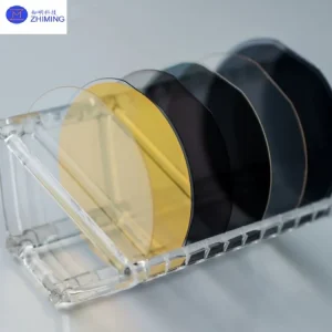
| Bề mặt hoàn thiện | SSP / DSP / CMP / MP |
| Chất lượng bề mặt | Sẵn sàng cho quá trình epitaxy (đã được mài bóng bằng phương pháp CMP) |
| Khoảng cách năng lượng | ~2,96 eV |
| Trọng tâm của ứng dụng | Cảm biến MEMS / Cảm biến tia UV / Quá trình phát triển graphene |
| Bao bì | Hộp đựng băng cassette hoặc hộp đựng tấm wafer đơn |
Các tùy chọn tùy chỉnh
Chúng tôi cung cấp các dịch vụ tùy chỉnh linh hoạt để đáp ứng các yêu cầu cụ thể về quy trình và ứng dụng. Các tùy chọn có sẵn bao gồm:
- Độ dày tấm wafer tùy chỉnh
- Các góc cắt thừa khác nhau (theo trục hoặc theo hướng tùy chỉnh)
- Kiểm soát nồng độ chất phụ gia và điện trở suất
- Bề mặt hoàn thiện và cấp độ đánh bóng
Điều này đảm bảo tính tương thích với các quy trình epitaksi và cấu trúc thiết bị khác nhau, cho dù là trong nghiên cứu, chế tạo mẫu thử hay sản xuất thử nghiệm.
Câu hỏi thường gặp
Câu hỏi 1: Thuật ngữ “epi-ready” có ý nghĩa gì đối với tấm wafer này?
A: Điều này có nghĩa là bề mặt tấm wafer đã được mài bóng chính xác bằng công nghệ CMP để đạt được độ nhám cực thấp, giúp nó có thể sử dụng ngay cho quá trình phát triển lớp phủ epitaxial mà không cần xử lý thêm.
Câu hỏi 2: Tại sao lại sử dụng 6H-SiC thay vì các dạng tinh thể khác?
A: 6H-SiC mang lại những lợi thế trong việc phát hiện tia cực tím, nuôi cấy graphene và các ứng dụng quang học nhờ khoảng cách năng lượng và cấu trúc tinh thể của nó.
Câu hỏi 3: Tấm wafer này có phù hợp cho sản xuất công nghiệp không?
A: Đúng vậy, các tấm wafer 6 inch được sử dụng rộng rãi trong sản xuất thử nghiệm và nghiên cứu phát triển (R&D) tiên tiến, tùy thuộc vào cấp độ chất lượng và yêu cầu ứng dụng.
Câu hỏi 4: Tôi có thể yêu cầu các thông số kỹ thuật tùy chỉnh không?
A: Vâng, chúng tôi hỗ trợ tùy chỉnh toàn diện, bao gồm độ dày, hướng, nồng độ tạp chất và xử lý bề mặt.
Tại sao nên chọn tấm wafer epitaxy SiC loại N 6H 6 inch này
Tấm wafer này được thiết kế để mang lại hiệu suất ổn định, chất lượng vật liệu cao và khả năng tương thích tuyệt vời với các quy trình bán dẫn tiên tiến. Đây là giải pháp lý tưởng cho các kỹ sư và nhà nghiên cứu đang tìm kiếm chất nền đáng tin cậy cho các ứng dụng MEMS, cảm biến tia UV và các công nghệ dựa trên graphene.

Đánh giá
Chưa có đánh giá nào.