

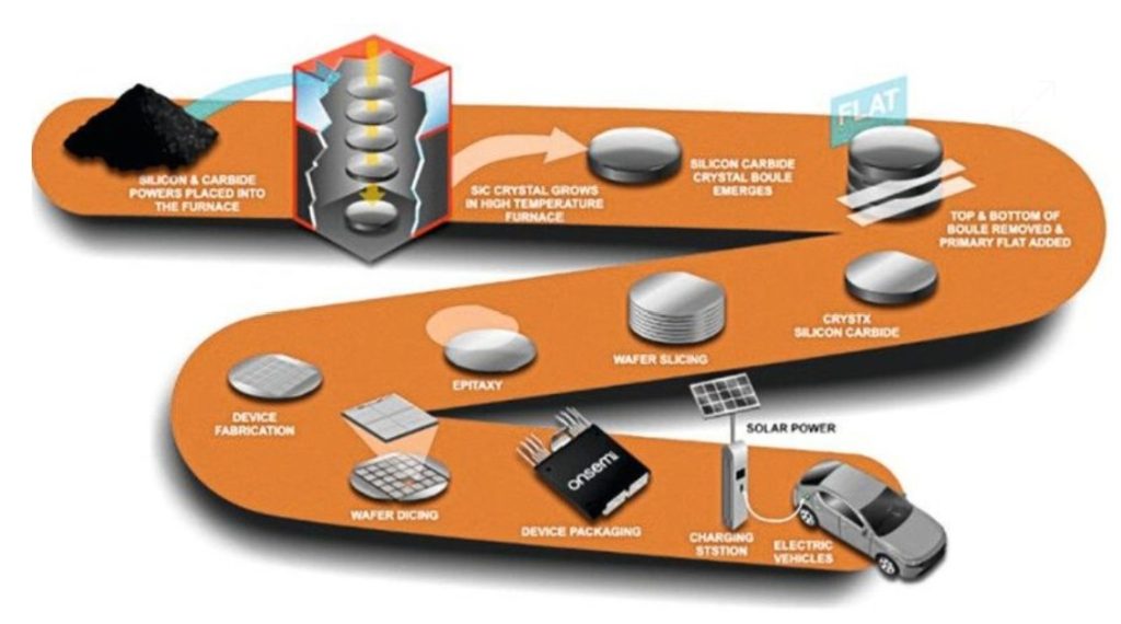
 رقاقة الرقاقة 6 بوصة N-Type 6H SiC Epitaxy Epitaxy Wafer 6 بوصة هي رقاقة أشباه الموصلات عالية الأداء مصممة للتطبيقات المتقدمة بما في ذلك أجهزة MEMS، وأجهزة الاستشعار بالأشعة فوق البنفسجية (UV)، ونمو الجرافين الفوقي. صُنعت هذه الرقاقة من بلورات أحادية كربيد السيليكون (SiC) عالية الجودة، وهي تجمع بين الخصائص الكهربائية والحرارية والميكانيكية الممتازة، مما يجعلها خيارًا مثاليًا للبيئات الصعبة حيث لا يمكن لمواد السيليكون التقليدية أن تعمل بشكل موثوق.
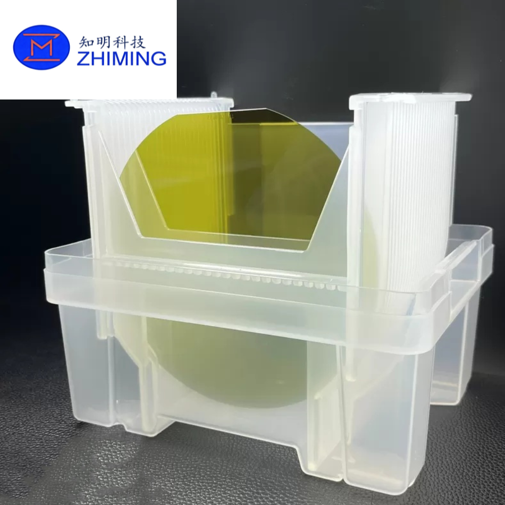
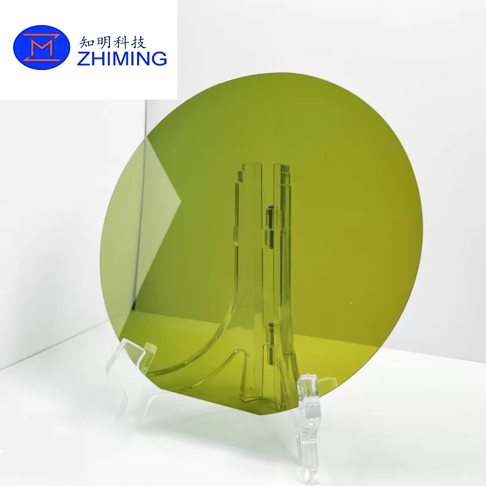
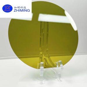
وبقطر قياسي يبلغ 150 مم (6 بوصة) وسُمك مضبوط بدقة يبلغ 350 ميكرومتر، توفر هذه الرقاقة ثباتًا ميكانيكيًا فائقًا وتوافقًا في العمليات مع معدات تصنيع أشباه الموصلات الحديثة. يتميز النوع المتعدد 6H بفجوة نطاق عريضة تبلغ 2.96 فولت تقريبًا، مما يتيح التشغيل الفعال في ظروف درجات الحرارة العالية والإشعاع العالي والظروف الكيميائية القاسية.
تتم معالجة كل رقاقة إلى سطح جاهز باستخدام تقنية التلميع الميكانيكي الكيميائي (CMP) المتقدمة. وهذا يضمن خشونة سطح منخفضة للغاية، والحد الأدنى من التلف تحت السطح، والظروف المثلى لعمليات نمو الطبقة الفوقية مثل الترسيب الكيميائي للبخار (CVD). والنتيجة هي تحسين أداء الجهاز، وزيادة الإنتاجية، وتعزيز الموثوقية للتطبيقات الحرجة.
 الميزات الرئيسية
سطح جاهز للنمو عالي الجودة من أجل نمو عالي الجودة
يتم تسليم الرقاقة بسطح مصقول كالمرآة يشبه المرآة CMP، مما يحقق خشونة دون النانومتر. ويضمن ذلك توافقًا ممتازًا مع عمليات النمو الفوق أكسجيني، خاصةً لتشكيل الجرافين وتصنيع الأجهزة الحساسة للأشعة فوق البنفسجية.
مُحسَّن لمعدات MEMS والبيئات القاسية
تُظهر رقاقة الرقاقة 6 بوصة من النوع N من النوع 6H SiC Epitaxy Epitaxy Wafer 6 بوصة ثباتًا حراريًا استثنائيًا، حيث تحافظ على الأداء في درجات حرارة تتجاوز 500 درجة مئوية. كما أن قوتها الميكانيكية العالية وخمولها الكيميائي يجعلها مناسبة لأجهزة MEMS التي تعمل في البيئات القاسية مثل أنظمة مراقبة الطيران والطاقة والصناعات.
فجوة نطاق عريضة لتطبيقات مستشعرات الأشعة فوق البنفسجية
مع وجود فجوة نطاق تبلغ 2.96 فولت تقريبًا، فإن هذه الرقاقة حساسة بشكل طبيعي للأشعة فوق البنفسجية بينما تظل غير حساسة للأطوال الموجية المرئية. وهذا ما يجعلها مثالية لمستشعرات الأشعة فوق البنفسجية العمياء الشمسية المستخدمة في الكشف عن اللهب والمراقبة البيئية وأنظمة الدفاع.
أداء كهربائي مستقر
يضمن التطعيم بالنيتروجين توصيلًا موثوقًا من النوع N، مما يتيح خصائص كهربائية متسقة وتكوين تلامس أومي مستقر. وهذا أمر ضروري لأجهزة الاستشعار الدقيقة والتطبيقات الإلكترونية الضوئية.
التوجيه البلوري المتحكم فيه
تتميز الرقاقة باتجاه خارج المحور بزاوية 4 درجات نحو (± 0.5 درجة)، مما يعزز النمو الفوقي التدريجي ويقلل من العيوب السطحية. وهذا يعزز التوحيد والتكرار أثناء تصنيع الجهاز.
التطبيقات
أجهزة MEMS في الظروف القاسية
تُستخدم رقاقة 6 بوصة N-Type 6H SiC Epitaxy Wafer 6 بوصة على نطاق واسع في مستشعرات MEMS مثل مستشعرات الضغط ومقاييس التسارع المصممة للبيئات ذات درجات الحرارة العالية والضغط العالي. هذه الأجهزة مهمة في التنقيب عن النفط والغاز، وأنظمة السيارات، ومراقبة التوربينات الفضائية.
مستشعرات الأشعة فوق البنفسجية الشمسية العمياء
تعتبر هذه الرقاقة مثالية لتصنيع أجهزة الكشف الضوئي بالأشعة فوق البنفسجية التي يمكنها الكشف بدقة عن الأشعة فوق البنفسجية دون تداخل من الضوء المرئي. هذه الإمكانية ضرورية لأنظمة الكشف عن اللهب وتقنيات الاستشعار البصري المتقدمة.
ركيزة نمو الجرافين
تعمل الرقاقة كركيزة عالية الجودة لنمو الجرافين الفوقي. وفي ظل ظروف التفريغ ذات درجة الحرارة المرتفعة، تتسامي ذرات السيليكون من سطح SiC، تاركةً وراءها طبقات الجرافين المرتبة جيدًا. تُستخدم هذه العملية على نطاق واسع في الإلكترونيات المتقدمة والأجهزة عالية السرعة والأبحاث الكمية.
الأنظمة الإلكترونية الضوئية المتقدمة
إن الشفافية البصرية والاستقرار المادي لمادة 6H-SiC تجعلها مناسبة للأجهزة الإلكترونية الضوئية المتخصصة، بما في ذلك الصمامات الثنائية الضوئية للأشعة فوق البنفسجية والمكونات عالية التردد.
المواصفات الفنية
| الممتلكات | المواصفات |
|---|---|
| المواد | الكريستال الأحادي SiC |
| القطر | 150 مم (6 بوصة) |
| السُمك | 350 ميكرومتر |
| متعدد الأنواع | 6H |
| نوع الموصلية | النوع N (المخدر بالنيتروجين) |
| التوجيه | 4 درجات باتجاه ± 0.5 درجة |
| تشطيب السطح | SSP / DSP / CMP / MPP |
| جودة السطح | جاهز للاستخدام (مصقول CMP) |
| فجوة النطاق | ~حوالي 2.96 فولت كهربي |
| تركيز التطبيق | MEMS / مستشعرات الأشعة فوق البنفسجية / نمو الجرافين |
| التعبئة والتغليف | كاسيت أو حاوية رقاقة واحدة أو حاوية رقاقة واحدة |
خيارات التخصيص
نحن نقدم خدمات تخصيص مرنة لتلبية متطلبات عملية وتطبيقات محددة. تشمل الخيارات المتاحة ما يلي:
- سماكة الرقاقة المخصصة
- زوايا القطع المختلفة (على المحور أو الاتجاه المخصص)
- تركيز المنشطات والتحكم في المقاومة المقاومة
- تشطيب السطح ودرجة التلميع
ويضمن ذلك التوافق مع مختلف العمليات الفوقية وهياكل الأجهزة، سواءً للأبحاث أو النماذج الأولية أو الإنتاج على نطاق تجريبي.
الأسئلة الشائعة
السؤال 1: ماذا تعني كلمة “جاهز للإيبي” بالنسبة لهذه الرقاقة؟
ج: هذا يعني أن سطح الرقاقة قد تم صقله بدقة باستخدام تقنية CMP لتحقيق خشونة منخفضة للغاية، مما يجعله مناسبًا على الفور للنمو الفوقي دون معالجة إضافية.
س2: لماذا تستخدم 6H-SiC بدلاً من الأنواع المتعددة الأخرى؟
ج: توفر 6H-SiC مزايا في الكشف عن الأشعة فوق البنفسجية ونمو الجرافين والتطبيقات البصرية بسبب فجوة النطاق والبنية البلورية.
س3: هل هذه الرقاقة مناسبة للإنتاج الصناعي؟
ج: نعم، تُستخدم الرقاقات مقاس 6 بوصات على نطاق واسع للإنتاج التجريبي والبحث والتطوير المتقدم، اعتمادًا على درجة الجودة ومتطلبات التطبيق.
س4: هل يمكنني طلب مواصفات مخصصة؟
ج: نعم، نحن ندعم التخصيص الكامل بما في ذلك السُمك والتوجيه والتطعيم والتشطيب السطحي.
لماذا تختار رقاقة الرقاقة الشمعية من النوع N من 6 بوصة 6H SiC Epitaxy Epitaxy Wafer 6 بوصة
تم تصميم هذه الرقاقة لتقديم أداء ثابت وجودة مواد عالية وتوافق ممتاز مع عمليات أشباه الموصلات المتقدمة. إنها حل مثالي للمهندسين والباحثين الذين يبحثون عن ركائز موثوقة لتقنيات MEMS والاستشعار بالأشعة فوق البنفسجية والتقنيات القائمة على الجرافين.


المراجعات
لا توجد مراجعات بعد.