
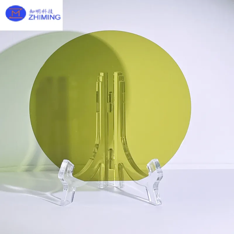
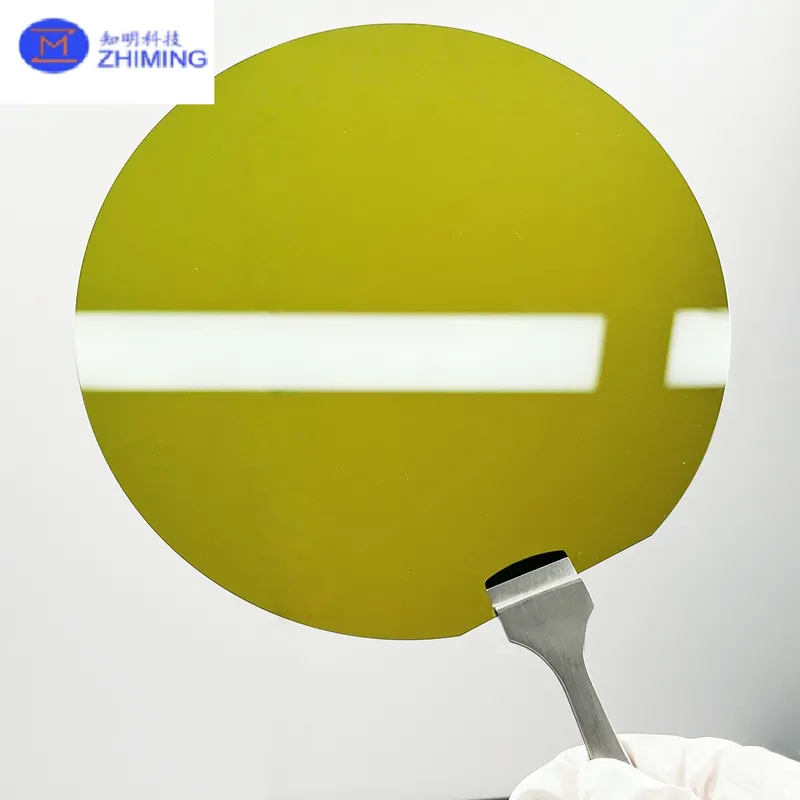
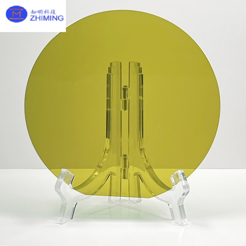

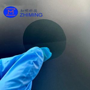
 The 4 inch 4H-N silicon carbide wafer is a conductive SiC substrate designed for advanced power semiconductor applications. It is based on the 4H crystal polytype, which is widely recognized in the industry for its superior electrical and thermal performance.
Silicon carbide belongs to the third-generation semiconductor materials and offers significant advantages over traditional silicon. Its wide bandgap, high breakdown electric field, and excellent thermal conductivity make it highly suitable for devices operating under high voltage, high frequency, and high temperature conditions.
This wafer is commonly used for manufacturing power devices such as MOSFETs, Schottky barrier diodes, JFETs, and IGBTs. These devices are critical components in modern energy systems, where efficiency, reliability, and compact design are essential. The 4 inch format provides a balance between cost efficiency and device yield, making it widely adopted in both research and industrial production environments.
Thông số kỹ thuật
| Tham số | Giá trị |
|---|---|
| Đường kính | 100 ± 0,5 mm |
| Độ dày | 350 ± 25 μm |
| Loại hình | 4H |
| Loại độ dẫn điện | Loại N |
| Độ nhám bề mặt | Ra ≤ 0.2 nm |
| TTV | ≤ 10 μm |
| Warp | ≤ 30 μm |
| Mật độ khuyết tật | MPD < 1 ea/cm² |
| Edge | 45° bevel, SEMI standard |
| Lớp | Sản xuất / Nghiên cứu / Mô hình |
These parameters ensure high surface quality and dimensional stability, which are essential for epitaxial growth and device fabrication processes.
Đặc tính vật liệu
Silicon carbide demonstrates a wide bandgap of approximately 3.26 eV, which allows devices to operate at significantly higher voltages compared to silicon. This results in improved power handling capability and reduced conduction losses.
Another important property is its high breakdown electric field, which can be nearly ten times greater than that of silicon. This enables thinner device structures and higher efficiency in power conversion systems.
Thermal conductivity is also a key advantage. SiC conducts heat about three times more effectively than silicon, allowing devices to maintain stable performance under high load conditions. This reduces the need for complex cooling systems and improves overall system reliability.
In addition, silicon carbide maintains stable electrical characteristics at temperatures exceeding 600°C. This makes it particularly suitable for applications in harsh environments such as automotive power systems, industrial drives, and aerospace electronics.
The material also offers high electron mobility and low on-resistance, contributing to faster switching speeds and reduced energy loss in power devices.
Available Wafer Sizes
Silicon carbide wafers are available in multiple diameters to meet different application needs:
| Size | Đường kính | Phạm vi độ dày |
|---|---|---|
| 2 inch | 50.8 mm | 330–350 μm |
| 3 inch | 76.2 mm | 350–500 μm |
| 4 inch | 100 mm | 350–500 μm |
| 6 inch | 150 mm | 350–500 μm |
| 8 inch | 200 mm | 350–500 μm |
Common types include conductive 4H-N, semi-insulating HPSI, and other specialized variants for RF and power applications.
Ứng dụng
In electric vehicles, SiC wafers are used in traction inverters, onboard chargers, and DC-DC converters. They improve energy efficiency, reduce heat generation, and enable more compact system designs.
In renewable energy systems, SiC devices are applied in solar inverters and wind power converters. Their high efficiency contributes to reduced energy loss and improved system performance.
Industrial systems also benefit from SiC technology, especially in high-power motor drives and automation equipment where reliability and durability are critical.
In power grid infrastructure, silicon carbide is used in smart grid systems and high-voltage transmission equipment to enhance energy conversion efficiency and reduce system losses.
Aerospace and defense applications utilize SiC for high-reliability electronics that must operate under extreme temperature and environmental conditions.
So sánh giữa Si và SiC
| Bất động sản | Silic | Cacbua silic |
|---|---|---|
| Khoảng cách năng lượng | 1,12 eV | 3.26 eV |
| Breakdown Field | Thấp | Cao |
| Độ dẫn nhiệt | Trung bình | Cao |
| Max Temperature | ~150°C | >600°C |
| Hiệu quả | Standard | Cao |
Silicon remains suitable for low-power and conventional electronics, while silicon carbide is increasingly preferred for high-power, high-efficiency systems.
Câu hỏi thường gặp
Q: What is the difference between silicon and silicon carbide wafers?
Tấm silicon được sử dụng rộng rãi trong các mạch tích hợp và các thiết bị điện tử tiêu chuẩn. Tấm cacbua silic được thiết kế dành cho lĩnh vực điện tử công suất, nơi đòi hỏi điện áp cao, nhiệt độ cao và hiệu suất cao.
Câu hỏi: SiC có những điểm khác biệt gì so với GaN?
SiC thường được sử dụng trong các ứng dụng điện áp cao và công suất lớn như xe điện và lưới điện. GaN phù hợp hơn cho các ứng dụng tần số cao và điện áp thấp, bao gồm các hệ thống tần số vô tuyến (RF) và thiết bị sạc nhanh.
Hỏi: Cacbua silic là gốm hay chất bán dẫn?
Cacbua silic vừa là vật liệu gốm vừa là chất bán dẫn. Vật liệu này kết hợp độ bền cơ học cao với các tính chất điện tuyệt vời, khiến nó trở nên phù hợp cho các ứng dụng điện tử đòi hỏi khắt khe.


Đánh giá
Chưa có đánh giá nào.