
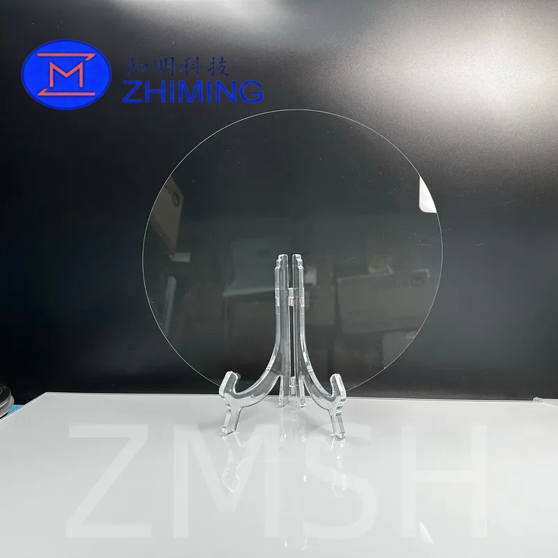

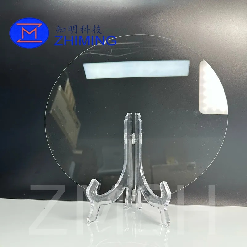
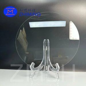
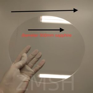
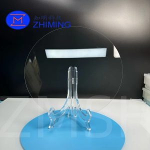
 The 12-inch sapphire wafer is a high-performance single-crystal aluminum oxide (Al₂O₃) substrate engineered for advanced semiconductor, optoelectronic, and high-temperature applications. It is manufactured from ultra-high purity sapphire crystal with a purity level of ≥99.99%, ensuring excellent structural uniformity and low defect density.
Sapphire is widely recognized for its exceptional mechanical hardness, chemical stability, and optical transparency, making it one of the most reliable substrate materials for extreme environments. The 12-inch format represents a high-end industrial-scale wafer size, designed for mass production of LED epitaxial layers and advanced electronic devices.
Unlike silicon, sapphire is an electrical insulator, which makes it particularly suitable for applications requiring high-frequency isolation, thermal stability, and optical transparency.
 Material Characteristics
Sapphire (α-Al₂O₃) is a single-crystal material with a unique combination of physical properties:
- Extremely high hardness (Mohs 9)
- Excellent resistance to thermal shock and high-temperature environments
- Outstanding chemical inertness against acids and alkalis
- Wide optical transmission range (UV to mid-infrared after polishing)
- High dielectric strength and electrical insulation
These properties make sapphire wafers a preferred choice in LED manufacturing, RF devices, laser systems, and aerospace-grade electronics.
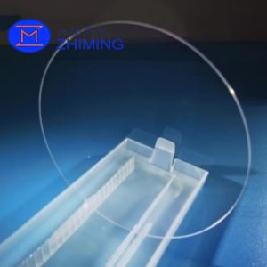
 Polishing & Surface Quality
This product supports both DSP (Double-Side Polishing) and SSP (Single-Side Polishing) processes, ensuring flexibility for different manufacturing requirements.
- Front surface: Epi-ready polishing (Ra < 0.3 nm)
- Back surface: Lapped or semi-polished depending on specification
- Surface cleanliness: Class 100 cleanroom processing
- Contamination control: ultra-low particle and metal residue levels
These surface qualities are critical for epitaxial growth processes such as MOCVD, MBE, and PECVD, where atomic-level surface uniformity directly impacts device performance.
Technical Specifications
| Parameter | Specification |
|---|---|
| Material | Single-crystal sapphire (Al₂O₃ ≥ 99.99%) |
| Diameter | 2” – 12” (customizable) |
| 12” Thickness | 3000 ± 20 μm |
| Orientation | C-plane (0001), A-plane, M-plane, R-plane |
| DSP / SSP | Available |
| OF Orientation | a-plane 0 ± 0.3° |
| TTV | ≤ 15 μm (12 inch) |
| BOW | -25 ~ 0 μm (12 inch) |
| Warp | ≤ 30 μm |
| Front Surface | Epi-ready (Ra < 0.3 nm) |
| Back Surface | Lapped (Ra 0.6–1.2 μm) |
| Packaging | Cleanroom vacuum packaging |
 Key Features
- Ultra-large 12-inch semiconductor-grade sapphire substrate
- High purity single-crystal Al₂O₃ (≥99.99%)
- Supports DSP and SSP polishing options
- Multiple crystallographic orientations available
- Excellent thermal stability and mechanical durability
- Ultra-low contamination cleanroom processing
- Suitable for high-end epitaxial growth and research applications
Applications
LED & Optoelectronics Manufacturing
C-plane sapphire wafers are widely used as substrates for GaN-based LED production, including blue, white, UV, and deep-UV devices.
Semiconductor Epitaxial Growth
Supports advanced epitaxial processes such as:
- MOCVD (Metal-Organic Chemical Vapor Deposition)
- MBE (Molecular Beam Epitaxy)
- PECVD (Plasma-Enhanced CVD)
RF & High-Frequency Devices
Used in heterojunction bipolar transistors (HBTs), laser diodes (LDs), and high-frequency communication components.
UV & Laser Applications
Sapphire substrates are suitable for UV detectors, laser windows, and photonic integration systems.
High-Temperature Electronics
Used as heat-resistant insulating substrates in high-power and high-frequency environments.
Customization Options
We provide flexible customization services for research and industrial production needs:
- Diameter: 1”, 2”, 3”, 4”, 6”, 8”, 12”
- Crystal orientation: C-plane / A-plane / M-plane / R-plane
- Off-angle adjustment available
- DSP / SSP surface treatment options
- Thickness and TTV optimization
- Edge shaping and chamfering
- Custom packaging (single wafer / cassette)
Each wafer is traceable with a unique serial number to ensure quality control and production traceability.
FAQ
Q1: What is the main advantage of sapphire wafers over silicon wafers?
Sapphire is transparent and electrically insulating, making it ideal for LED and optical applications, while silicon is mainly used for electronic circuits.
Q2: Why is 12-inch sapphire wafer important?
It supports large-scale industrial LED and semiconductor production, improving efficiency and reducing per-unit cost in mass manufacturing.
Q3: What does DSP and SSP mean?
DSP refers to Double-Side Polishing, while SSP refers to Single-Side Polishing. These affect surface quality and application suitability.
Q4: Can sapphire wafers be used directly for devices?
They are used as substrates and require epitaxial growth or additional processing before final device fabrication.
Q5: Why is sapphire used in LEDs?
Because it provides a stable lattice structure for GaN growth and excellent thermal and optical performance.

Reviews
There are no reviews yet.