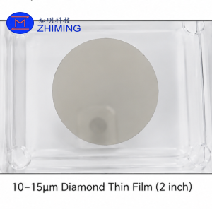
SiC Manufacturing Solutions
Crystal growth, wafer slicing, laser processing, and bonding solutions for SiC power semiconductor devices and compound semiconductors.

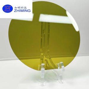
Sapphire Processing Solutions
High-precision crystal growth and laser processing equipment for sapphire wafers used in LED, optoelectronics, and optical components.

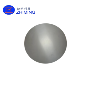
Silicon Wafer Solutions
Solutions for silicon crystal growth, wafer slicing, and precision processing, supporting R&D, pilot production, and volume manufacturing.

Laser Precision Processing Solutions
Laser drilling and cutting solutions for wafers, glass, sapphire, and SiC, enabling micron-level precision and low thermal impact.

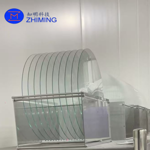
Wafer Cutting & Slicing Solutions
Wire sawing and precision cutting equipment for wafer slicing with high accuracy, low material loss, and stable performance.

R&D & Customized Solutions
Flexible equipment configurations and engineering support tailored for research institutes, pilot lines, and process development.
-
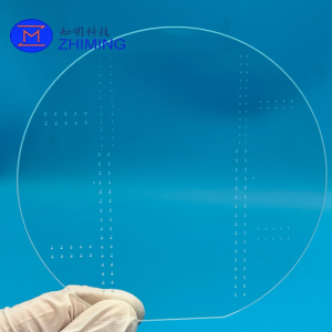
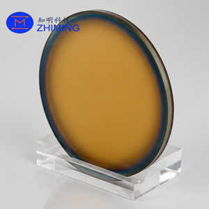
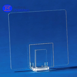
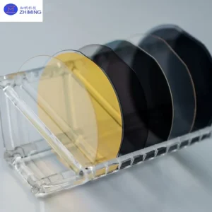
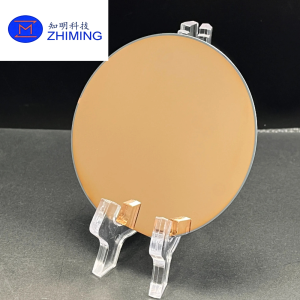
Semiconductor Consumables
Sapphire Temporary Wafer Carrier for Advanced Semiconductor Packaging
Read more -
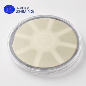
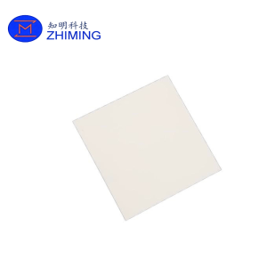
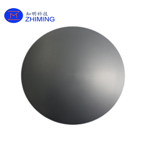
Semiconductor Consumables
CVD Silicon Carbide (SiC) Electrode for Semiconductor Plasma Systems
Read more