
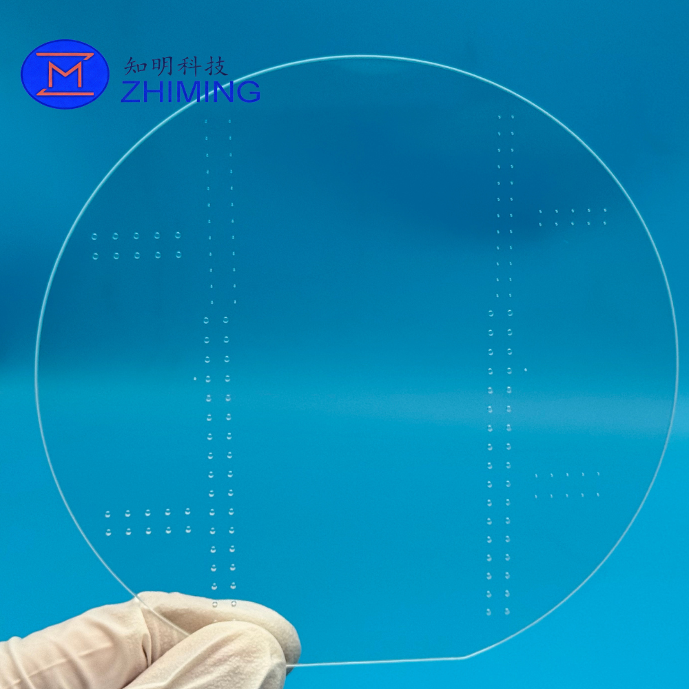
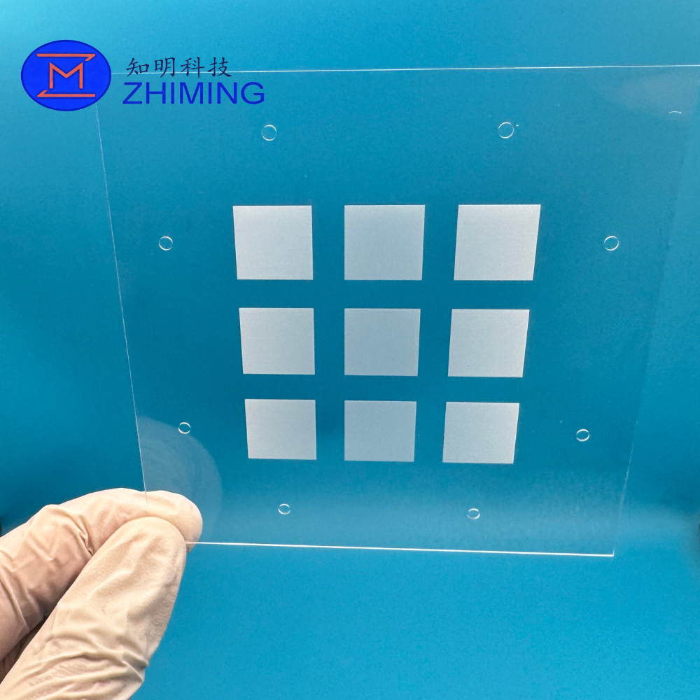
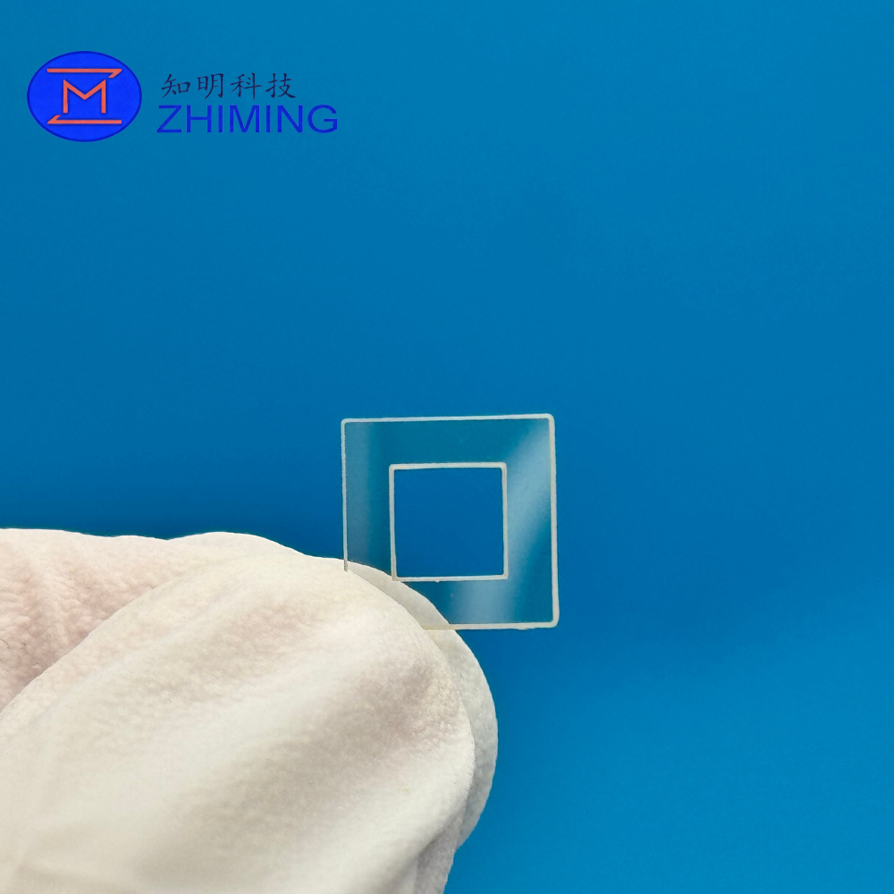
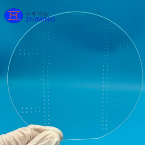
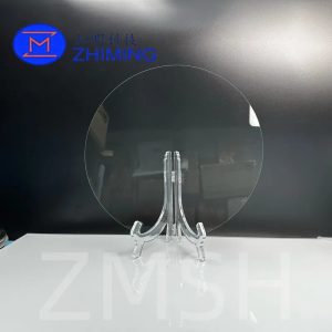
 This product is a custom sapphire substrate with TGV structures, manufactured through precision cutting, drilling, polishing and micro-pattern processing. The through holes can be arranged as single vias, dense via arrays, functional openings or special patterns depending on the device design.
Compared with standard glass substrates, sapphire offers better scratch resistance, stronger mechanical durability and higher dimensional stability. It is especially suitable for demanding environments where the substrate must remain transparent, clean, stable and resistant to heat or chemical exposure.
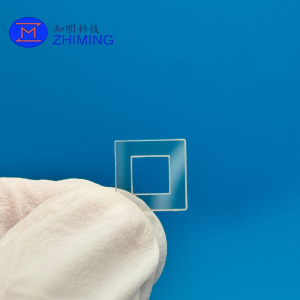
We support customized production based on drawings, including round sapphire wafers, square sapphire plates, rectangular substrates and special-shaped sapphire parts.
Main Advantages
| Advantage | Description |
|---|---|
| High-Strength Sapphire Material | Excellent hardness and mechanical durability |
| Precision TGV Processing | Through-hole arrays, micro vias and patterned openings available |
| Good Optical Transparency | Suitable for optical, photonic and inspection-related applications |
| Chemical Resistance | Stable in many harsh processing environments |
| Electrical Insulation | Suitable for electronic and semiconductor-related substrate use |
| Custom Design Support | Size, thickness, hole layout and pattern can be made to order |
| Clean Surface Finish | Polished surface options available for precision applications |
Available Custom Options
| Item | Options |
|---|---|
| Material | Single crystal sapphire / Al₂O₃ |
| Shape | Round, square, rectangular, customized shape |
| Structure | Through holes, micro vias, square holes, patterned windows |
| Hole Arrangement | Single hole, multiple holes, via array, custom pattern |
| Surface Finish | SSP / DSP / polished surface |
| Edge Type | Straight edge, chamfered edge, beveled edge |
| Processing Method | Laser drilling, cutting, grinding, polishing |
| Drawing Support | PDF, CAD, DXF, STEP or sample-based customization |
Typical Applications
Semiconductor Packaging
TGV sapphire substrates can be used in advanced packaging research, wafer-level packaging, interposer structures and vertical interconnection design. The through-hole layout can be customized to meet different packaging and alignment requirements.
MEMS and Sensor Devices
Sapphire substrates with micro holes or square openings are suitable for MEMS components, pressure sensors, optical sensors, micro-structured devices and precision testing platforms.
Optical and Photonic Components
Because sapphire has good transparency and high stability, it can be used in optical windows, laser modules, photonic packaging, imaging systems and inspection equipment.
High-Reliability Electronic Components
Sapphire provides strong electrical insulation and dimensional stability, making it suitable for selected electronic, RF and high-frequency device applications.
Customized Research and Prototype Projects
For R&D projects, we can provide small-batch sapphire substrates with different via sizes, hole patterns, thicknesses and surface requirements.
 Why Use Sapphire for TGV Structures?
TGV technology requires accurate through-hole processing and stable substrate performance. Sapphire is a strong candidate when the application needs more than ordinary glass can provide.
Its key benefits include:
High hardness and wear resistance
Good dimensional stability
Excellent thermal resistance
Strong chemical durability
Good optical transparency
Reliable electrical insulation
Suitable for precision microstructure processing
For applications involving harsh environments, optical inspection, microelectronic packaging or long-term device reliability, sapphire can provide a more durable substrate solution.
 Manufacturing Capability
We provide customized sapphire TGV substrate processing according to customer drawings and project requirements.
Our processing capabilities include:
Precision sapphire wafer cutting
Sapphire plate shaping
Through-hole drilling
Micro via array processing
Square window and cavity machining
Double-side polishing
Edge grinding and chamfering
Custom pattern processing
Prototype and batch production
Information Needed for Quotation
To provide an accurate quotation, please share the following details:
Substrate size or wafer diameter
Thickness requirement
Hole diameter
Hole quantity
Hole spacing / pitch
Hole position drawing
Surface finish requirement
Tolerance requirement
Quantity
Application or working environment
If drawings are available, please send CAD, DXF, STEP or PDF files for technical evaluation.
FAQ
Q1: Can you make custom hole arrays on sapphire substrates?
Yes. We can process single holes, multiple holes, dense hole arrays, square holes and custom patterns according to customer drawings.
Q2: What is the difference between sapphire TGV and glass TGV?
Sapphire has higher hardness, stronger wear resistance, better thermal stability and excellent chemical durability. It is suitable for applications requiring higher reliability than ordinary glass.
Q3: Can the sapphire substrate be made into square or rectangular shapes?
Yes. We can supply round wafers, square plates, rectangular substrates and customized shapes.
Q4: Is this product suitable for optical applications?
Yes. Sapphire has good optical transparency and is widely used in optical windows, sensors, photonic devices and inspection systems.
Q5: Do you support small-batch samples?
Yes. Small-batch prototype production is available for testing, R&D and design verification.

Reviews
There are no reviews yet.