
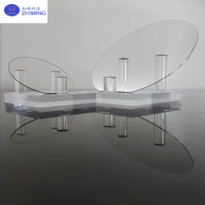
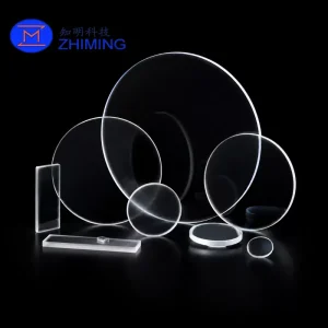
 The 4 inch HPSI silicon carbide wafer is a high-purity semi-insulating substrate engineered for advanced RF, microwave, and optoelectronic applications. HPSI refers to high purity semi-insulating material, characterized by extremely high resistivity and excellent electrical isolation.
Silicon carbide is a wide bandgap semiconductor composed of silicon and carbon. Compared with conventional silicon wafers, it offers superior thermal conductivity, higher breakdown electric field, and better performance under extreme operating conditions. In semi-insulating form, SiC significantly reduces parasitic conduction, making it an ideal platform for high-frequency and high-power electronic devices.
This 4 inch wafer format is widely used in both research and industrial production due to its balance of cost, maturity, and process compatibility. It is especially suitable for RF devices, 5G communication systems, radar modules, and emerging optical technologies such as AR waveguide components.
Specifications
| Parameter | Value |
|---|---|
| Diameter | 100 ± 0.5 mm |
| Thickness | 350 μm |
| Material | SiC single crystal |
| Type | HPSI (semi-insulating) |
| Resistivity | ≥1E5 to ≥1E10 ohm·cm |
| Surface Roughness | CMP Ra ≤ 0.2 nm |
| TTV | ≤ 10 μm |
| Warp | ≤ 30 μm |
| Orientation | On-axis <0001> or off-axis options |
| Edge | Standard SEMI bevel |
| Grade | Production / Research / Dummy |
These parameters ensure high surface quality, low defect density, and stable mechanical properties required for epitaxial growth and precision device fabrication.
Material Characteristics
Silicon carbide is one of the most important third-generation semiconductor materials. Its wide bandgap enables devices to operate at higher voltages with lower leakage currents compared to silicon.
For HPSI wafers, the defining feature is their extremely high resistivity. This property minimizes unwanted current flow within the substrate, which is critical for maintaining signal integrity in RF and microwave applications.
Thermal conductivity is significantly higher than that of traditional semiconductor materials, allowing efficient heat dissipation during high-power operation. This reduces thermal stress and improves long-term reliability.
SiC also exhibits a high breakdown electric field, enabling devices to handle high voltage without increasing size. In addition, the material maintains stable performance under high temperature, high frequency, and radiation exposure, making it suitable for demanding environments.
Applications
RF and Microwave Devices
HPSI silicon carbide wafers are widely used as substrates for RF amplifiers and high-frequency circuits. Their high resistivity reduces parasitic losses and improves signal transmission efficiency, making them essential for advanced communication electronics.
5G Communication Infrastructure
In 5G systems, devices operate at higher frequencies and require materials with excellent electrical isolation. HPSI SiC wafers support stable performance in base stations and wireless modules, enabling higher data transmission efficiency and reduced energy loss.
AR Glasses and Optical Systems
In augmented reality devices, SiC wafers are used in optical and waveguide-related components. Their structural stability and compatibility with precision processing technologies support the development of compact and high-performance optical systems.
Radar and Defense Systems
HPSI SiC substrates are suitable for radar and defense electronics that require high power, high frequency, and reliability. They maintain stable operation under extreme environmental conditions, including high temperature and radiation.
Optoelectronic Devices
These wafers are also used in optoelectronic and photonic devices where electrical isolation and thermal performance are critical for device efficiency and stability.

Available Grades
Production grade
Used for commercial device manufacturing with strict quality control and low defect density.
Research grade
Suitable for laboratory development, testing, and process optimization.
Dummy grade
Applied in equipment calibration, process testing, and non-functional use.
Si vs SiC Comparison
| Property | Silicon | Silicon Carbide |
|---|---|---|
| Bandgap | 1.12 eV | ~3.26 eV |
| Resistivity | Low | Very high (HPSI) |
| Thermal Conductivity | Moderate | High |
| Frequency Capability | Limited | Excellent |
| Application Focus | Logic and IC | RF and high-frequency |
Silicon remains dominant in conventional electronics, while silicon carbide is increasingly used in high-frequency and high-performance systems.
FAQ
Q: What is an HPSI silicon carbide wafer?
An HPSI wafer is a high purity semi-insulating silicon carbide substrate with very high electrical resistivity, designed for RF, microwave, and optoelectronic applications.
Q: Why is high resistivity important?
High resistivity reduces parasitic conduction and signal interference, which is critical for maintaining efficiency and signal integrity in high-frequency devices.
Q: Is silicon carbide suitable for optical applications?
Yes, silicon carbide can be used in certain optical and photonic applications due to its thermal stability and compatibility with advanced fabrication processes.
Reviews
There are no reviews yet.