
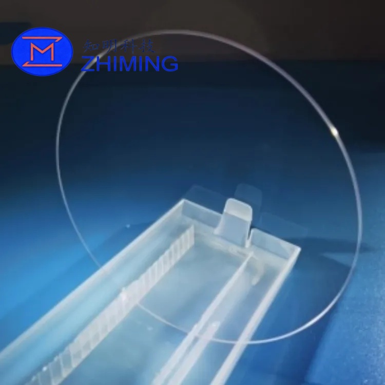
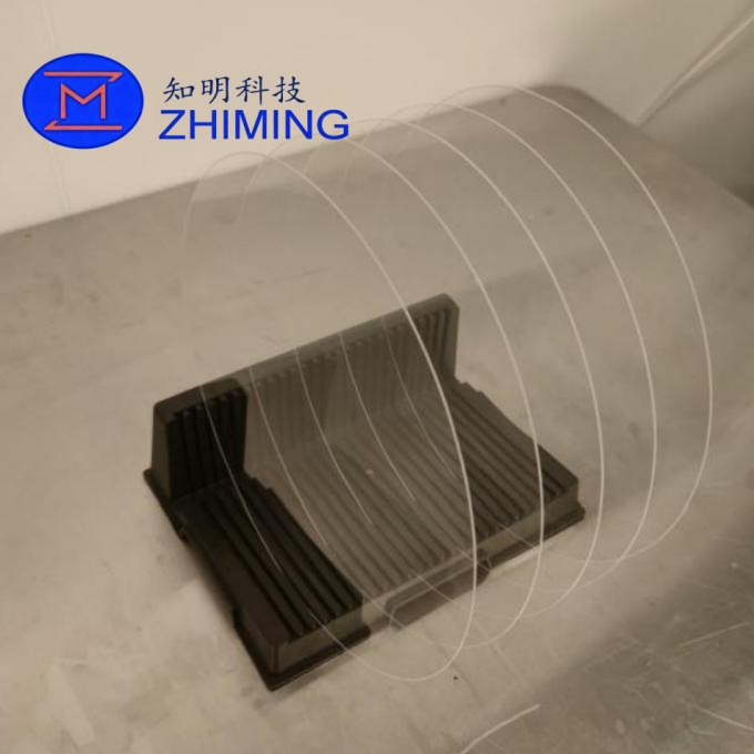
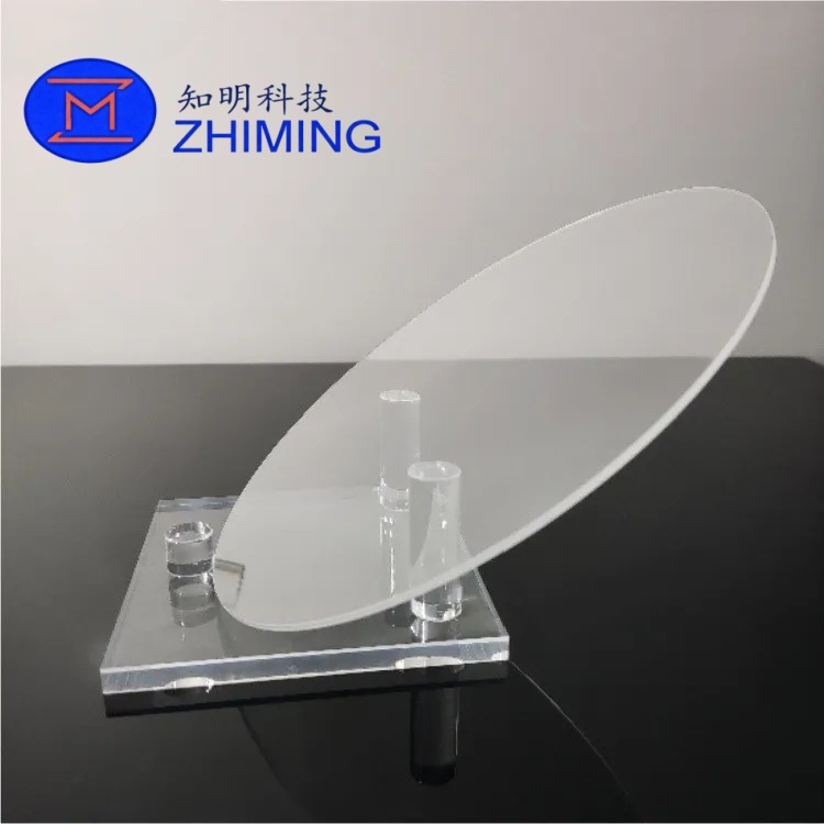
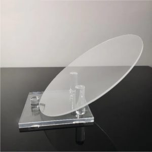
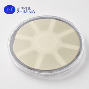
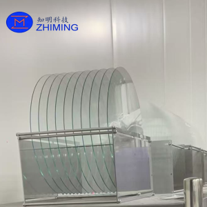
 The 8-inch fused quartz wafer is a premium high-purity synthetic quartz (SiO₂ ≥99.99%) substrate engineered for high-precision applications in semiconductor, MEMS, optical, and laser systems. Its ultra-low thermal expansion, exceptional UV-IR transmittance, and excellent chemical resistance make it ideal for demanding environments such as photolithography, etching, thin-film deposition, and high-precision sensor fabrication.
Each wafer is carefully produced under stringent quality control in a cleanroom environment to ensure superior flatness, surface finish, and purity. This guarantees reliable performance for critical industrial, research, and aerospace applications.
Key Features & Advantages
-
Ultra-High Purity (≥99.99%): Minimizes contamination in semiconductor and optical processes.
-
Exceptional Thermal Stability: Softening point ~1683°C, short-term tolerance up to 1450°C for high-temperature processes.
-
Ultra-Low Thermal Expansion (0.55 × 10⁻⁶/K): Ensures dimensional stability under thermal stress.
-
Superior Optical Transmission: UV-IR range 185 nm–2.5 µm, ideal for photolithography, laser optics, and UV sensors.
-
High Surface Quality: Ra ≤1.0 nm and TTV ≤10 µm for uniform thin-film deposition and precise sensor integration.
-
Chemical Resistance: Resistant to most acids (except HF) and alkalis, suitable for wet etching and harsh environments.
-
Radiation Resistance & Dielectric Stability: Supports aerospace and high-energy physics applications.
-
Customizable Shapes & Sizes: Round, square, annular, or sector-shaped wafers with optional polishing, AR/IR/DLC coatings, and microfabrication.
Applications
| Industry | Application | Benefit |
|---|---|---|
| Semiconductor | Photomask substrates, etching carriers, CMP polishing pads | High-temperature stability, ultra-low defects, ensures chip manufacturing precision |
| Photovoltaics | PECVD process wafers, thin-film deposition substrates | Thermal shock resistance, improves solar cell efficiency |
| Optoelectronics | LED/LD substrates, laser windows, optical sensors | High UV-IR transmission, low autofluorescence, enhances device performance |
| Precision Optics | Lens substrates, prisms, beam splitters, IR windows | Low thermal expansion, high homogeneity, ensures optical stability |
| Research & Lab | Synchrotron radiation, VUV experiments, high-energy detectors | Radiation-resistant, withstands extreme conditions |
| Aerospace | Satellite optical windows, high-temperature observation panels | Thermal shock endurance, space-grade reliability |
Technical Specifications
| Parameter | Specification |
|---|---|
| Material | Synthetic Fused Quartz (SiO₂ ≥99.99%) |
| Diameter | 200 mm (8-inch) |
| Thickness Range | 100 µm – 3000 µm (customizable) |
| Total Thickness Variation (TTV) | ≤10 µm |
| Surface Roughness (Ra) | ≤1.0 nm |
| Total Impurity Content | ≤2.0 µg/g |
| Thermal Expansion Coefficient | 0.55 × 10⁻⁶/K (20–300°C) |
| Temperature Resistance | Softening Point 1683°C, short-term up to 1450°C |
| UV Transmittance | >90% (200–260 nm) |
| Surface Flatness | High precision, TTV ≤10 µm |
| Shape Options | Round (standard), custom shapes available |
| Certifications | RoHS, ISO9001 |
 FAQ
FAQ
-
Q: What is the standard thickness of an 8-inch quartz wafer?
A: Standard thickness is 0.5–1.0 mm, with custom options up to 10 mm for specialized semiconductor and optical applications. -
Q: Why choose fused quartz wafers over silicon wafers?
A: Fused quartz wafers provide superior UV transparency, higher thermal stability (up to 1730°C), chemical resistance, and dimensional stability, making them ideal for high-precision lithography and harsh processes. -
Q: Can FUYAO provide custom wafer shapes and surface treatments?
A: Yes. Options include round, square, annular, sector-shaped wafers, with surface treatments such as optical polishing, AR/IR/DLC coatings, drilling, and grooving.
Request a Quote for 8-Inch High-Purity Fused Quartz Wafer (200mm) for Precision Sensors and Optical Applications
Tell us your required specifications, dimensions, quantity, application and technical requirements. You can also provide drawings or additional project information. Our technical team will review your requirements and reply as soon as possible.

Reviews
There are no reviews yet.