


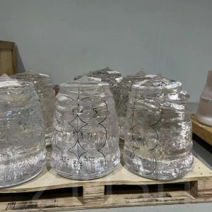
 Sapphire wafer blanks are high-purity, as-cut single-crystal aluminum oxide (Al₂O₃) substrates derived directly from sapphire boules using advanced wire-sawing technology. Unlike finished wafers, these substrates are delivered in their raw and unprocessed state, meaning the surface retains saw marks and has not undergone lapping, polishing, or chemical mechanical planarization (CMP).
This form of sapphire is widely used as the starting material in semiconductor, optical, and high-temperature engineering industries, where downstream users require full control over surface finishing, crystallographic orientation alignment, and thickness precision.
Sapphire (α-Al₂O₃) is one of the hardest known engineered materials, ranking 9 on the Mohs hardness scale, second only to diamond. It exhibits excellent resistance to abrasion, thermal shock, and chemical corrosion, making it highly suitable for extreme processing environments. These properties allow sapphire wafer blanks to serve as a stable base material in both industrial production lines and advanced research laboratories.
 Material Characteristics
Sapphire wafer blanks are composed of single-crystal aluminum oxide with purity ≥ 99.99%, ensuring high structural consistency and minimal impurity-induced lattice defects. This is critical for applications involving epitaxial growth or optical transmission.
Key material properties include:
- High hardness and scratch resistance
- Excellent thermal conductivity and stability at high temperatures
- Strong resistance to acids, alkalis, and plasma environments
- Wide optical transmission range (UV to IR after polishing)
- High mechanical strength under stress and vibration conditions
These characteristics make sapphire wafer blanks particularly valuable in environments where silicon or glass substrates fail under stress or temperature limitations.
 Manufacturing Process
Sapphire wafer blanks are produced through a controlled industrial process:
- Crystal Growth – Sapphire boules are grown using methods such as Kyropoulos or heat exchange techniques, ensuring large single-crystal ingots with controlled defect density.
- Orientation Cutting – Boules are precisely aligned according to crystallographic planes (C-plane, A-plane, R-plane, M-plane).
- Wire Saw Slicing – The ingot is sliced into wafer-shaped blanks using diamond wire saws, resulting in as-cut surfaces.
- Cleaning & Inspection – Each wafer blank is inspected for cracks, edge integrity, and thickness uniformity.
At this stage, the product is intentionally left unpolished to serve as a flexible raw material for downstream manufacturing processes.
Key Features
- Ultra-high purity single-crystal sapphire (≥99.99% Al₂O₃)
- Available in standard semiconductor wafer sizes: 2”, 3”, 4”, 6”, 8”
- Custom thickness range from 0.5 mm to 3.0 mm or beyond
- Multiple crystal orientations for different optical and electronic applications
- Raw wire-sawn surface ideal for custom lapping and CMP processing
- High structural stability under mechanical and thermal stress
- Consistent quality suitable for industrial-scale manufacturing
Applications
Sapphire wafer blanks serve a broad range of advanced industries due to their mechanical strength and chemical stability.
Semiconductor and LED Industry
Sapphire wafer blanks are commonly used as substrates for GaN-based LED epitaxial growth. After polishing, they provide a highly stable platform for producing high-efficiency optoelectronic devices such as blue and UV LEDs.
Optical and Photonic Systems
After precision finishing, sapphire is used in optical windows, laser cavities, infrared imaging systems, and sensor covers, where high transparency and scratch resistance are essential.
Research and Development
Universities and material science laboratories utilize sapphire wafer blanks for CMP process development, surface engineering studies, and crystal defect analysis.
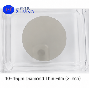
Thin Film Deposition
The material is widely used as a base substrate for ALD, PVD, and CVD deposition experiments, especially in early-stage research where surface roughness is not yet critical.
Industrial and Aerospace Applications
With additional machining, sapphire wafers can be transformed into high-temperature structural components, protective sensor covers, and precision mechanical spacers.
Technical Specifications
| Parameter | Specification |
|---|---|
| Material | Single-crystal sapphire (Al₂O₃) |
| Purity | ≥ 99.99% |
| Crystal Structure | Alpha-phase sapphire |
| Shape | Circular wafer blank |
| Diameter | 2”, 3”, 4”, 6”, 8” (custom available) |
| Thickness | 0.5 – 3.0 mm (customizable) |
| Orientation | C-plane (0001), A-plane, R-plane, M-plane |
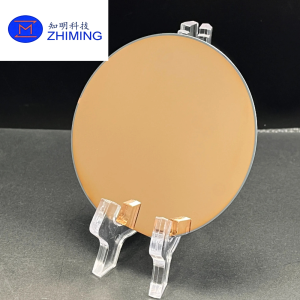
| Surface Condition | As-cut / wire-sawn (unpolished) |
| Edge Condition | Rough edge (standard), chamfer optional |
Advantages
Sapphire wafer blanks offer several strategic advantages compared to fully processed wafers:
First, they provide a cost-efficient raw material solution, reducing upfront material costs for manufacturers who prefer in-house finishing. Second, they allow complete flexibility in defining final wafer properties, including thickness tolerance, surface roughness, and flatness.
Third, they are ideal for process development and pilot production lines, where experimentation and iterative optimization are required. Finally, sapphire maintains its intrinsic mechanical strength and thermal resilience even in raw form, ensuring reliability throughout downstream processing.
Industry Context & Quality Considerations
In semiconductor manufacturing, the quality of the final wafer is strongly influenced by the initial crystal quality and cutting precision. Sapphire wafer blanks provide a stable foundation for achieving high-yield epitaxial growth when processed under controlled CMP conditions.
Industry standards typically require strict control of:
- Surface flatness after polishing
- Subsurface damage depth after slicing
- Crystal orientation accuracy within tight angular tolerances
- Defect density for optical and electronic applications
By starting from a high-quality wafer blank, manufacturers can better control these downstream variables.
FAQ
Q1: What is a sapphire wafer blank used for?
It is used as a raw substrate for semiconductor, LED, optical, and research applications after further processing.
Q2: How is it different from a polished sapphire wafer?
A wafer blank is unpolished and retains saw-cut surfaces, while a polished wafer is ready for direct device fabrication.
Q3: Can dimensions be customized?
Yes, diameter, thickness, orientation, and edge finishing can all be customized according to technical requirements.
Q4: Is it suitable for direct LED production?
No. It must undergo lapping and polishing before being used for epitaxial LED growth.
Q5: What makes sapphire better than glass or quartz?
Sapphire offers significantly higher hardness, temperature resistance, and chemical stability compared to conventional optical materials.
Reviews
There are no reviews yet.