
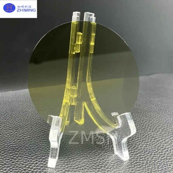
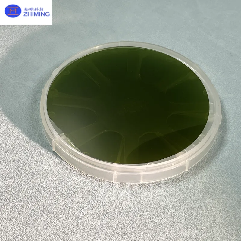
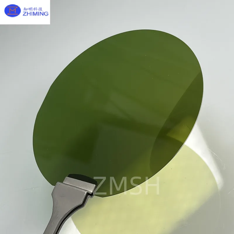
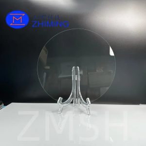
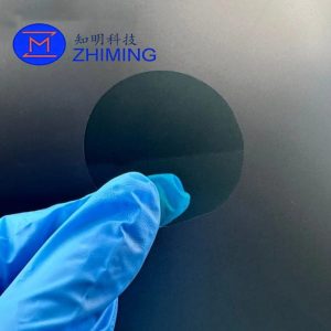
 The 8 inch SiC epitaxial wafer represents the latest advancement in wide bandgap semiconductor technology. Built on a 200 mm SiC substrate with a high-quality epitaxial layer, this product is designed to support scalable, high-efficiency power device manufacturing.
Compared with smaller wafer sizes, 8 inch SiC wafers significantly increase usable area, enabling higher device output per wafer and reducing cost per chip. This makes them a critical solution for industries transitioning to large-scale production of silicon carbide power devices.
SiC epitaxial wafers combine the intrinsic advantages of silicon carbide, including wide bandgap, high breakdown electric field, and excellent thermal conductivity, with precisely controlled epitaxial layers tailored for device fabrication. These wafers are widely used in next-generation MOSFETs, Schottky diodes, and integrated power modules.
Key Specifications
| Parameter | Value |
|---|---|
| Diameter | 200 ± 0.5 mm |
| Polytype | 4H-SiC |
| Conductivity Type | N-type |
| Thickness | 700 ± 50 μm |
| Surface Finish | Double-side CMP polished |
| Orientation | 4.0° off-axis ±0.5° |
| Notch | Standard notch orientation |
| Edge Profile | Chamfer / Rounded edge |
| Surface Roughness | Sub-nanometer level |
| Packaging | Cassette or single wafer container |
Typical resistivity:
- N-type: 0.015–0.028 Ω·cm
- Semi-insulating: ≥1E7 Ω·cm
Grades available:
- Zero MPD grade
- Production grade
- Research grade
- Dummy grade
 Epitaxial Layer Capabilities
The epitaxial layer is grown using advanced chemical vapor deposition (CVD) technology, enabling precise control of thickness, doping concentration, and uniformity.
Available customization includes:
- N-type or P-type epitaxial layers
- Adjustable epi thickness for different device structures
- Uniform doping profiles across the full wafer
- Low defect density for high device yield
High-quality epitaxy is essential for achieving stable electrical performance and long-term reliability in power devices.
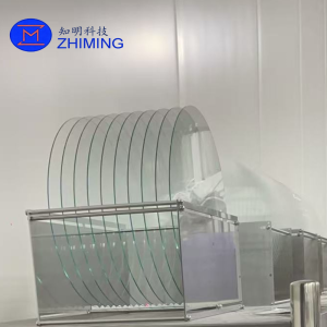
 Manufacturing Process
Substrate Preparation
High-purity monocrystalline SiC substrates are produced using high-temperature growth methods and polished to achieve ultra-low surface roughness.
Epitaxial Growth
The epitaxial layer is deposited at high temperature using CVD systems, ensuring uniform thickness and consistent material properties across the 200 mm wafer.
Doping Control
Precise doping is applied during epitaxial growth to meet the requirements of different device architectures.
Metrology and Inspection
Each wafer undergoes comprehensive testing, including surface analysis, defect mapping, and electrical characterization to ensure consistent quality.
Advantages
Scalable Manufacturing
The 8 inch wafer size significantly increases chip output per wafer, improving production efficiency and reducing cost per device.
High Efficiency Performance
SiC material properties enable lower switching losses, higher power density, and improved energy efficiency.
Excellent Thermal Management
High thermal conductivity supports stable operation under high power conditions and reduces cooling requirements.
Low Defect Density
Advanced crystal growth and epitaxial processes ensure high yield and reliable device performance.
Future-Ready Platform
8 inch SiC wafers are aligned with the semiconductor industry trend toward larger wafer formats and automated mass production.

Applications
Electric Vehicles
Used in traction inverters, onboard chargers, and DC-DC converters. Larger wafer size supports mass production of high-efficiency power devices for EV platforms.
Renewable Energy Systems
Applied in solar inverters and wind power converters, where efficiency and reliability are critical for long-term operation.
Industrial Power Electronics
Supports motor drives, automation systems, and high-power equipment requiring stable and efficient energy conversion.
5G and RF Infrastructure
Enables high-frequency and high-power RF components used in communication systems and base stations.
Consumer Power Electronics
Used in compact, high-efficiency power supplies and fast charging systems.
FAQ
Q1: What is the main advantage of 8 inch SiC wafers?
The larger wafer size increases the number of chips per wafer, significantly reducing manufacturing cost per device and improving production efficiency.
Q2: Is 8 inch SiC technology mature?
It is currently transitioning from pilot production to early-stage mass production, with increasing adoption in advanced semiconductor manufacturing.
Q3: Can epitaxial layers be customized?
Yes, doping type, thickness, and electrical properties can be tailored to meet specific device requirements.
Q4: Are existing production lines compatible with 8 inch wafers?
Some equipment upgrades may be required, but many modern fabs are already preparing for 200 mm SiC processing.

Reviews
There are no reviews yet.