
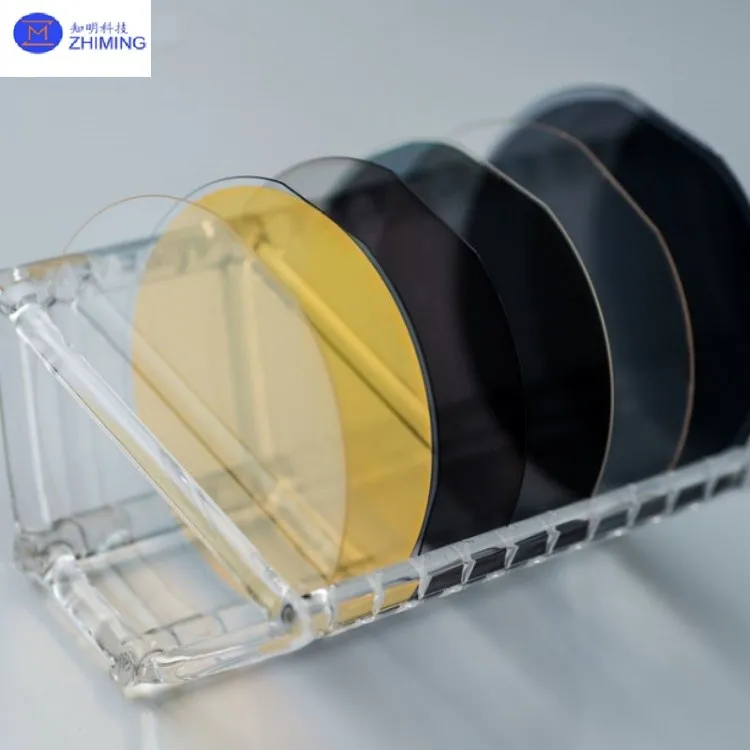

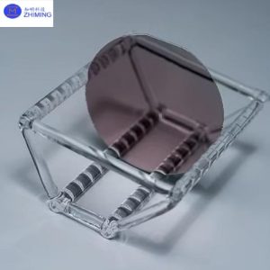
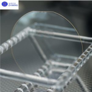
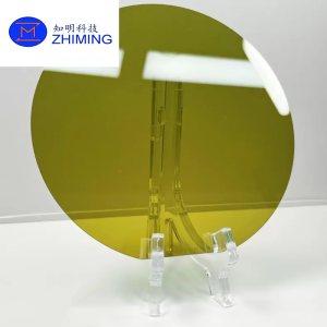
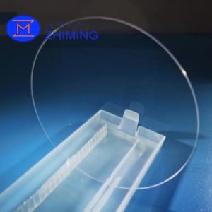
 A szigetelőn elhelyezett vékonyrétegű lítium-niobát (LNOI) szeletek fejlett fotonikus hordozók, amelyeket integrált optikai, mikrohullámú fotonikus és kvantumrendszerekben használnak.
A szerkezet egy SiO₂ szigetelőrétegre rögzített, szilícium-aljzaton nyugvó, egykristályos lítium-niobát vékonyrétegből áll.
Ez a konfiguráció erős optikai bezárást, rendkívül alacsony terjedési veszteséget és magas elektro-optikai hatékonyságot biztosít, ami az integrált fotonika egyik legfontosabb platformjává teszi.
Mi az a vékonyrétegű lítium-niobát (TFLN)?
A vékonyrétegű lítium-niobát (TFLN) egy mikrométernél kisebb kristályos LiNbO₃ réteget jelöl, amelyet optikai hullámvezető és elektrooptikai alkalmazásokhoz fejlesztettek ki.
A hagyományos lítium-niobáttal összehasonlítva a TFLN szűkebb optikai korlátozást, kisebb eszközméretet és nagyobb integrációs sűrűséget tesz lehetővé.
A TFLN-t általában LNOI-szilíciumlapkákra építik fel, hogy egy teljes integrált fotonikus platformot hozzanak létre.
 Fő jellemzők
- Rendkívül alacsony optikai veszteség < 0,05 dB/cm 1550 nm-en
- Magas elektro-optikai együttható (r₃₃ akár 90 pm/V)
- Kompatibilitás szubmikronos hullámvezetőkkel (<1 μm)
- CMOS-kompatibilis integráció Si/SiN platformokkal
- Kiváló hőstabilitás (kb. 1140 °C-os Curie-hőmérséklet)
- Többféle kristálycsiszolás: X-csiszolás / Y-csiszolás / Z-csiszolás
- Szilíciumlapka-méretek: 3 hüvelyk / 4 hüvelyk / 6 hüvelyk / 8 hüvelyk
Oszlop szerkezete
| Réteg | Anyag | Funkció |
|---|---|---|
| Felső réteg | LiNbO₃ vékonyréteg (TFLN) | Elektro-optikai és nemlineáris optikai funkciók |
| Középső réteg | SiO₂ (beágyazott oxid) | Optikai szigetelés és korlátozás |
| Alsó réteg | Cínium / Kvarc / Zafír | Mechanikai támogatás és CMOS-kompatibilitás |
Műszaki specifikációk
A szelet műszaki adatai
| Paraméter | Érték |
|---|---|
| A szelet átmérője | 3″, 4″, 6″, 8″ |
| Teljes vastagság | 525 ± 25 μm |
| Íj | ±50 μm |
| Warp | <50 μm |
| LTV | <1,5 μm (5×5 mm², 95%) |
Vékonyrétegű lítium-niobát réteg
| Paraméter | Érték |
|---|---|
| Anyag | Egykristályos LiNbO₃ |
| Vastagság | 300 nm – 1000 nm |
| Iránymeghatározás pontossága | ±0,5° |
| Felületi érdesség | Ra < 1 nm |
| Kötési hibák | 1 mm-nél nagyobb hibák nincsenek |
Beágyazott oxidréteg (SiO₂)
| Paraméter | Érték |
|---|---|
| Anyag | SiO₂ |
| Vastagság | 100 nm – 2 μm (testreszabható) |
| Egyenletesség | ±5% |
 Gyártási folyamat
Az LNOI-szeleteket félvezetőipari minőségű eljárásokkal gyártják:
- Ionbeültetés a rétegek szabályozott elválasztásához
- Oszlopok rögzítése szigetelő hordozókra
- Magas hőmérsékletű hőkezelés a kristályok stabilizálása érdekében
- Kémiai-mechanikus polírozás (CMP) a felület kiegyenlítéséhez
- Végső optikai és szerkezeti minőség-ellenőrzés
Főbb alkalmazási területek
- Nagy sebességű optikai adatátvitel (100G–800G modulátorok)
- Kvantumfotonika (összefonódott fotonok előállítása, QKD-rendszerek)
- Mikrohullámú fotonika (rádiófrekvenciás jelfeldolgozás, milliméteres hullámhosszú rendszerek)
- Nemlineáris optika (frekvenciakonverzió, optikai fésűk)
- Integrált érzékelőrendszerek (biokémiai és optikai rezonátorok)
Teljesítménybeli előny a tömeges LiNbO₃-hoz képest
| Ingatlan | LiNbO₃ ömlesztett formában | LNOI vékonyréteg |
|---|---|---|
| Optikai veszteség | Magasabb | <0,05 dB/cm |
| Integráció | Alacsony | Nagy sűrűségű fotonika |
| A készülék mérete | Nagy | mikron alatti méret |
| CMOS-kompatibilitás | Nem | Igen |
| Modulációs hatékonyság | Mérsékelt | Magas (Vπ ~1 V elérhető) |
Testreszabási lehetőségek
| Opció | Leírás |
|---|---|
| Kristályvágás | X-vágás / Y-vágás / Z-vágás |
| Filmvastagság | 300 nm – 1000 nm |
| Hordozóanyag | Cínium / Kvarc / Zafír |
| Oxidréteg | 100 nm – 2 μm (egyedi) |
| Dopping | MgO-val adalékolt LiNbO₃ kapható |
Minőségellenőrzés
| Tesztfeladat | Módszer |
|---|---|
| Optikai veszteség | Hullámvezető terjedési vizsgálat |
| Felületi érdesség | AFM-mérés |
| Vastagság egyenletessége | Térképrendszer |
| A kötés minősége | IR-vizsgálat |
| Laposság | Oszlopmérnöki mérés |
Mérnöki szakértelem
ZMSH teljes körű támogatást nyújt az LNOI-szilíciumlapok fejlesztéséhez:
- Vékonyréteg-tervezés optimalizálása
- A szilíciumlapok összekapcsolásának technológiai tervezése
- Fotonikus eszközök gyártásának támogatása
- Nanofabrikáció (EBL / IBE)
- Optikai teljesítmény vizsgálata és validálása
Alkalmas mind a kutatás-fejlesztési prototípusok gyártására, mind pedig a legfeljebb 8 hüvelykes szilíciumlapkák kis sorozatú gyártására.
GYIK
Mire szolgál az LNOI?
Az LNOI-lemezeket széles körben használják az optikai kommunikációban, a kvantumfotonikában, a nemlineáris optikában és az integrált fotonikus áramkörökben.
Mekkora a vékonyréteg jellemző vastagsága?
A lítium-niobát vékonyrétegek vastagsága általában 300 nm és 1000 nm között mozog.
Miért érdemes az LNOI-t használni a tömeges lítium-niobát helyett?
Az LNOI alacsonyabb optikai veszteséget, nagyobb integrációs sűrűséget és CMOS-kompatibilis fotonikus integrációt kínál.
Az LNOI integrálható-e a szilícium-fotonikával?
Igen, az LNOI teljes mértékben kompatibilis a szilícium- és szilícium-nitrid fotonikus platformokkal.

Értékelések
Még nincsenek értékelések.