
In 300mm semiconductor manufacturing, wafer notching and coring are critical mechanical processes used to prepare silicon wafers for downstream fabrication steps. These processes ensure proper wafer orientation, structural integrity, and compatibility with automated handling systems in advanced fabs.
As wafer sizes continue to increase and process nodes become more advanced, precision in mechanical wafer shaping has become increasingly important for yield control and equipment compatibility.
This article explains what wafer notching and coring are, how they are performed, and why they are essential in modern semiconductor production.
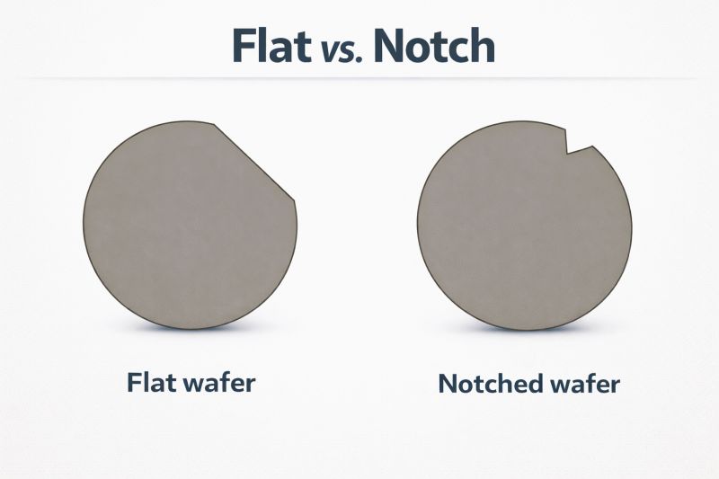
What Is Wafer Notching?
Wafer notching is the process of creating a small, precisely positioned cut (notch) on the edge of a silicon wafer. This notch serves as an orientation reference for automated systems.
Purpose of Wafer Notching
The primary functions of wafer notching include:
- Crystal orientation alignment (e.g., <100> or <111> silicon orientation)
- Equipment positioning reference for robotic handling systems
- Process consistency across lithography, etching, and deposition steps
- Automation compatibility in 300mm fabs
In 300mm wafers, the notch is a standardized feature that allows equipment to identify wafer orientation without manual intervention.
What Is Wafer Coring?
Wafer coring refers to the removal or shaping of the central region or edge sections of a wafer for specialized applications or process requirements. While less commonly discussed than notching, coring plays a role in specific advanced manufacturing and research applications.
Key Functions of Wafer Coring
- Creating central alignment or mechanical relief structures
- Preparing wafers for specialized bonding or stacking processes
- Removing stressed or defective central regions in experimental processes
- Supporting custom wafer geometries for research and prototyping
In advanced semiconductor environments, coring is typically performed with high-precision diamond tools or laser-assisted systems.
Equipment Used in Notching and Coring
High-precision wafer shaping requires specialized equipment designed for micron-level accuracy and minimal damage.
1. Precision Wafer Notching Systems
These systems use diamond grinding wheels or laser-based cutting heads to form accurate notches on wafer edges.
2. Diamond Wire Saws
Used in some coring and shaping applications, especially when dealing with hard materials or thick wafers.
3. Laser Micromachining Systems
Advanced fabs may use laser-based tools for non-contact notching and coring to reduce mechanical stress.
4. CNC Precision Grinding Machines
Provide high repeatability and tight dimensional control for wafer edge processing.
Process Flow in 300mm Wafer Manufacturing
A simplified process flow for wafer notching and coring includes:
- Wafer Inspection
- Surface defect detection
- Thickness and flatness measurement
- Orientation Alignment
- Determining crystal axis direction
- Setting notch reference position
- Mechanical or Laser Processing
- Notch cutting on wafer edge
- Coring or central shaping (if required)
- Deburring and Surface Finishing
- Removal of micro-cracks and debris
- Edge polishing for stress reduction
- Post-Process Inspection
- Optical metrology
- Dimensional verification
- Surface integrity check
Importance in 300mm Semiconductor Manufacturing
As wafer diameter increases to 300mm and beyond, mechanical precision becomes more critical due to:
1. Automation Requirements
Modern fabs rely heavily on robotic wafer handling. Even slight misalignment can cause:
- Wafer breakage
- Misplacement in lithography tools
- Yield loss in downstream processes
2. Stress Sensitivity
Large wafers are more sensitive to mechanical stress introduced during edge processing. Poor notching or coring can lead to:
- Micro-cracks
- Edge chipping
- Delamination during thermal cycling
3. Process Integration
Notches must be precisely aligned with:
- Lithography alignment systems
- Etching tool orientation
- Metrology reference frameworks
Common Challenges in Wafer Notching and Coring
1. Edge Chipping
Improper cutting parameters can cause micro-fractures at the wafer edge, affecting mechanical strength.
2. Subsurface Damage
Excessive mechanical force may introduce hidden defects that propagate during thermal processing.
3. Alignment Errors
Even small deviations in notch position can affect full fab automation systems.
4. Tool Wear
Diamond tools degrade over time, affecting consistency and requiring strict maintenance control.
Quality Control and Inspection Methods
To ensure reliability in semiconductor production, wafer notching and coring processes are tightly controlled using:
- Optical microscopy inspection
- Laser scanning metrology
- Edge profile measurement systems
- Surface roughness analysis (AFM/SEM in advanced cases)
These methods ensure compliance with semiconductor-grade standards.
Industry Applications
Wafer notching and coring are widely used in:
- 300mm silicon wafer manufacturing
- Advanced logic and memory fabs
- Research and development wafer prototyping
- Specialty semiconductor materials (SiC, sapphire, glass wafers)
Conclusion
Wafer notching and coring are essential precision processes in 300mm semiconductor manufacturing. Although they may appear minor compared to lithography or deposition, these mechanical steps directly influence wafer handling accuracy, process stability, and overall yield.
As semiconductor technology continues to advance, demand for ultra-precise edge processing will continue to grow, making these processes increasingly important in next-generation fabs.