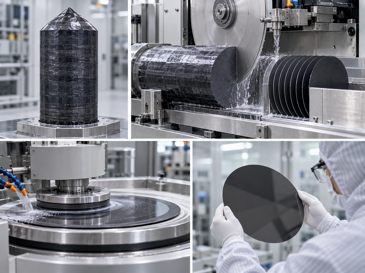
Industry News 300mm SiC Wafers Move Closer to Reality: Crystal Growth, Slicing, Grinding and Dicing Challenges for Next-Generation Semiconductors Read More »
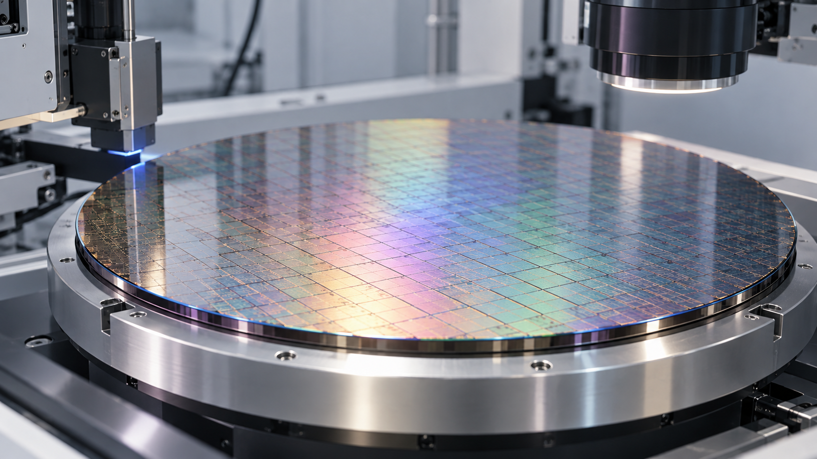
Company News Global 300mm Fab Equipment Spending Jumps 31% in 2026: What the Expansion Means for Dummy Wafers, Wafer Handling and Process Equipment Read More »
Company News AI Advanced Packaging Accelerates in 2026: Why Temporary Wafer Carriers, Wafer Thinning and Hybrid Bonding Matter More Than Ever Read More »
Industry News 300mm Epitaxial Silicon Wafers for Advanced Logic: Epi Thickness, Resistivity, Defect Density and Edge Specifications Read More »
Industry News Wafer Plating for Advanced Semiconductor Manufacturing: Seed Layer Uniformity, Edge Exclusion and Backside Metallization Read More »
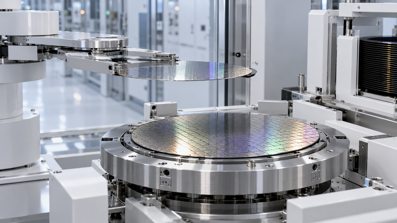
Industry News Designing Wafer Handling Stages for 300mm Automated Fabs: Vacuum Chuck Flatness, Edge Grip, Particle Control and Robot Handoff Read More »
Industry News 6-Inch β-Ga₂O₃ Wafers Arrive: Can Gallium Oxide Become the Next Scalable Ultra-Wide-Bandgap Substrate? Read More »
Industry News Single-Crystal AlN Substrates in 2026: Why 100mm AlN Is Opening a New Path for GaN RF Devices Read More »
Industry News 300mm Photonics-SOI Is Moving Into Mass Production: What AI Optical Interconnects Require From SOI Wafers Read More »
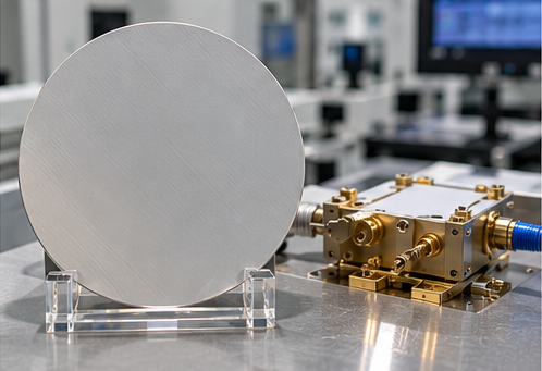
SiC Beyond Power Electronics: Why High-Thermal-Conductivity SiC Is Being Explored for AI Packaging and Heat Spreading Read More »