LNOI / TFLN Wafer Selection Guide for Integrated Photonics: X-Cut vs Z-Cut, LN Film Thickness, BOX, Handle Substrate and Surface Quality Read More »
Industry News SOI Wafer Thickness Guide: Device Layer, BOX Thickness, Handle Wafer and Selection for MEMS, RF and Silicon Photonics Read More »
Industry News Diamond-Copper Composite Heat Spreaders: Thermal Conductivity, CTE Matching and AI/HPC Packaging Applications Read More »
Technology & Applications Dummy Wafer vs Reclaim Wafer vs Test Wafer: Selection Guide for Equipment Qualification and Process Development Read More »
Industry News Wafer Handling End-Effector Selection Guide: Vacuum, Edge-Grip, Bernoulli and Non-Contact Handling for Fragile Wafers Read More »
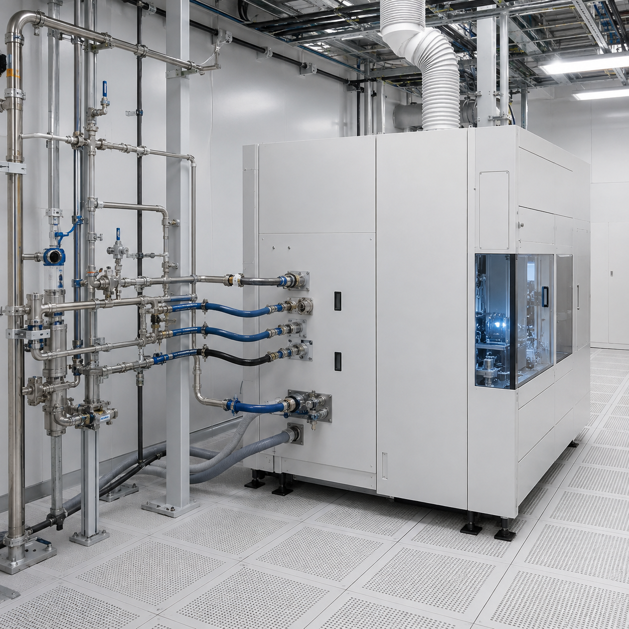
Industry News Semiconductor Equipment Utility Requirements Guide: Power, CDA, Cooling Water, Exhaust, Vacuum and Floor Loading Read More »
Industry News Black Quartz Glass: High-Absorption Quartz for Semiconductor Thermal Management and Optical Shielding Read More »
Industry News 300mm Wafer Notch Specification Guide: Dimensions, Orientation, Measurement and Dicing Alignment Read More »
Industry News 300mm Glass Wafer Dicing Guide: Blade Selection, Chipping Control, Kerf Width, TTV and Cleaning Requirements Read More »
Quartz Chamber Components in Fluorine vs. Chlorine Plasma: Etch Rate, Surface Damage, Particle Generation and Service Life Read More »