
Silicon carbide (SiC), a representative material of the third-generation semiconductor family, has emerged as a cornerstone for next-generation power electronics, high-frequency devices, and advanced optical systems. Driven by the transition from 8-inch to 12-inch wafers and early-stage exploration of 14-inch substrates, the SiC industry is undergoing a structural transformation from isolated technological breakthroughs to fully integrated supply chain optimization.
This article provides a comprehensive and academic overview of recent advancements in SiC crystal growth, wafer processing equipment, metrology systems, substrate and epitaxial materials, as well as auxiliary process technologies. It further analyzes how wafer size scaling reshapes cost structures, manufacturing efficiency, and global competitiveness.
1. Introduction: The Strategic Role of Silicon Carbide
In modern semiconductor technology, wide bandgap materials are redefining the limits of device performance. Among them, SiC stands out due to its superior physical and electronic properties, including:
- Wide bandgap (~3.26 eV)
- High critical electric field (~10× silicon)
- Excellent thermal conductivity (~3× silicon)
- Strong radiation and chemical resistance
These characteristics make SiC indispensable in applications such as electric vehicles, renewable energy systems, data centers, and emerging optical technologies.
Two dominant trends define the current evolution of the SiC industry:
- Wafer size expansion (6-inch → 8-inch → 12-inch → 14-inch)
- Transition from fragmented innovation to full supply chain integration
By 2026, the industry is entering a critical phase where laboratory-scale achievements are being translated into high-volume manufacturing capabilities.
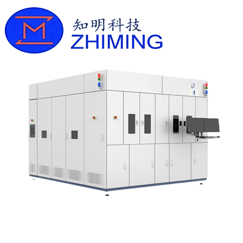
2. Crystal Growth Equipment: The Foundation of the SiC Value Chain
2.1 Physical Vapor Transport (PVT) as the Mainstream Technology
The dominant method for SiC single crystal growth is Physical Vapor Transport. Unlike silicon, SiC cannot be grown from a melt due to its extremely high sublimation temperature. Instead, solid SiC source material sublimates at high temperature and recrystallizes onto a seed crystal.
Key technical challenges in scaling to 12-inch crystals include:
- Maintaining thermal stability above 2000°C
- Controlling temperature gradients across large diameters
- Ensuring uniform vapor transport
- Achieving long-duration process stability
The successful transition to 12-inch crystal growth marks a pivotal shift toward industrial-scale manufacturing comparable to the silicon ecosystem.
2.2 Alternative Approaches: Liquid Phase Growth
In addition to PVT, Liquid Phase Epitaxy and related liquid-phase growth techniques are gaining attention. These approaches offer:
- Lower defect densities
- Improved dopant incorporation control
- Advantages in p-type material growth
Although still in development, liquid-phase methods may complement PVT in high-performance and specialized applications.
2.3 Thermal Field Engineering and Defect Control
The quality of SiC crystals is highly sensitive to thermal field distribution. Advanced systems now incorporate:
- Multi-zone heating configurations
- Real-time thermal feedback control
- Coupled thermal-fluid simulations
These innovations significantly reduce defects such as micropipes and dislocations, which directly affect device yield and reliability.
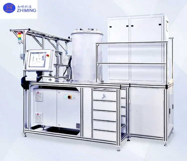
3. Wafer Processing Equipment: Precision Manufacturing for Hard and Brittle Materials
SiC is one of the hardest semiconductor materials, approaching a Mohs hardness scale value of 9. This creates substantial challenges in wafer processing.
3.1 Thinning Technology: Achieving Sub-Micron Uniformity
Wafer thinning is essential for device fabrication and thermal management. Key advancements include:
- Thickness variation control within 1 μm
- Ultra-precision air-bearing spindles
- Vacuum or electrostatic wafer handling systems
The integration of thinning with laser-based layer separation processes reduces material loss by up to 30%, significantly improving cost efficiency.
3.2 Dicing and Cutting: Efficiency and Yield Optimization
Two primary cutting approaches are used:
- Multi-wire sawing for ingots
- Dicing for processed wafers
Recent innovations focus on:
- Increasing throughput per tool
- Reducing kerf loss
- Minimizing edge chipping and subsurface damage
These improvements are critical for scaling production to meet growing demand in power electronics.
3.3 Laser-Based Separation Technologies
Laser processing technologies, including laser lift-off and water-guided laser cutting, are becoming essential for advanced SiC manufacturing.
Advantages include:
- Non-contact processing
- Reduced mechanical stress
- Higher material utilization
These methods are particularly important for ultra-thin wafers and heterogeneous integration.
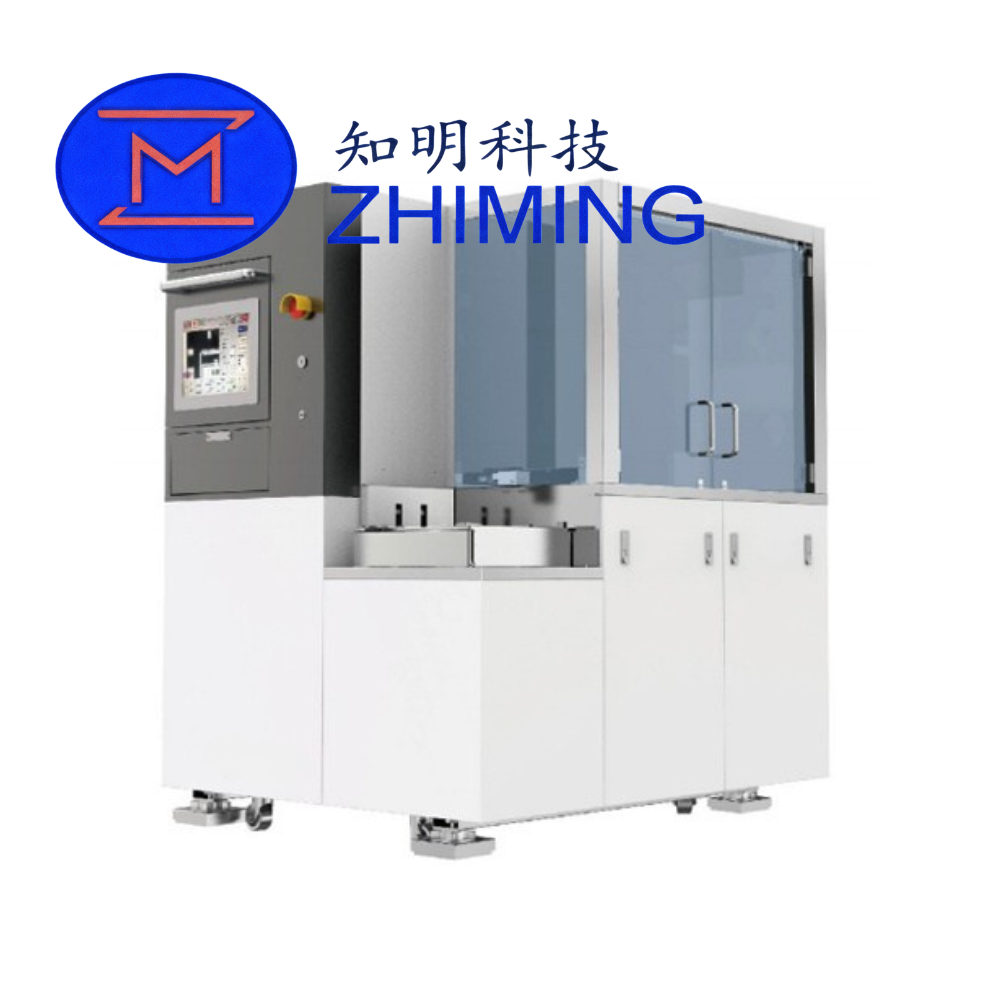
4. Metrology and Inspection: Enabling Yield Control
Inspection systems serve as the “eyes” of semiconductor manufacturing. High-end SiC metrology focuses on:
- Surface defect detection
- Subsurface damage analysis
- Epitaxial layer uniformity measurement
Recent progress in domestic metrology technologies has narrowed the gap with global leaders, enabling more precise process control and higher yield rates.
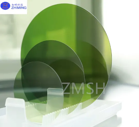
5. Substrates and Epitaxy: From Size Scaling to Quality Optimization
5.1 Substrate Development: 12-Inch Maturity and 14-Inch Exploration
The transition to larger wafers significantly improves manufacturing efficiency:
- Compared to 6-inch wafers: >3× chip output
- Compared to 8-inch wafers: ~2.25× increase
- Estimated cost reduction: ~40%
Meanwhile, early-stage 14-inch crystal development indicates the next frontier in wafer scaling.
5.2 Epitaxial Growth: The Final Step for Device Performance
Epitaxy forms the active layer of semiconductor devices. Advanced SiC epitaxial processes achieve:
- Thickness uniformity <3%
- Doping uniformity ≤8%
- Device yield >96%
The integration of epitaxy equipment with substrate production represents a key step toward full process optimization.
5.3 Emerging Optical Applications
Beyond power electronics, SiC is expanding into optical applications due to its high refractive index and transparency.
One notable innovation involves gradient-structured optical gratings, enabling:
- Full-color waveguide displays
- Simplified optical architectures
- Higher efficiency in AR/VR systems
This opens new opportunities in consumer electronics and advanced imaging technologies.
6. Supporting Materials and Advanced Packaging
6.1 Polishing and Slurry Technologies
High-performance polishing slurries are essential for achieving defect-free surfaces. Innovations include:
- Multi-modal particle dispersion
- Chemically modified abrasives
- Reduced subsurface damage
These technologies are crucial for both substrate preparation and optical applications.
6.2 Thermal Management in Advanced Packaging
With increasing power density in AI and high-performance computing, thermal management has become a critical challenge.
SiC offers significant advantages due to its high thermal conductivity, making it a promising candidate for:
- Heat spreaders
- Interposer materials
- Advanced packaging substrates
Future packaging architectures may increasingly incorporate SiC to improve performance and reliability.
7. Global Landscape and Future Outlook
7.1 Intensifying Competition in Large-Diameter Wafers
The global race toward 12-inch and beyond is accelerating. Key trends include:
- Parallel development of 8-inch mass production and 12-inch R&D
- Increasing investment in large-scale fabrication facilities
- Growing emphasis on vertical integration
7.2 From Size Scaling to Cost Transformation
Looking ahead, several trends are expected to shape the SiC industry:
- Mass production of 12-inch wafers (2026–2027)
- Expansion into new applications such as AI data centers and AR devices
- Diversification of growth and processing technologies
- Transition from equipment import to global export capabilities
8. Conclusion
The SiC semiconductor industry is undergoing a profound transformation driven by wafer size scaling and full supply chain integration. From breakthroughs in 12-inch crystal growth to early exploration of 14-inch substrates, and from sub-micron precision processing to advanced epitaxial technologies, each innovation contributes to a more mature and competitive ecosystem.
As manufacturing technologies continue to evolve, SiC is poised to transition from a niche material for high-end applications to a mainstream semiconductor platform. The convergence of equipment innovation, material science, and process engineering will ultimately define the pace of this transition.
In this context, wafer size is no longer just a technical parameter—it represents efficiency, cost advantage, and strategic positioning in the global semiconductor landscape.