
Semiconductor manufacturing is one of the most sophisticated industrial systems, characterized by extreme precision, high capital intensity, and complex process integration. Equipment plays a foundational role across the entire production flow, directly determining process capability, device performance, yield, and cost efficiency. This article presents a structured and academic overview of semiconductor manufacturing equipment, focusing on the eight major fabrication steps and the five core front-end tool categories. It aims to provide a comprehensive understanding of how equipment technologies enable modern integrated circuit production.
1. Industry Structure and the Role of Equipment
The semiconductor industry is typically divided into three segments:
- Upstream: materials and equipment
- Midstream: wafer fabrication
- Downstream: packaging, testing, and applications
Among these, equipment represents the most technologically intensive segment. It serves as the enabling infrastructure for all fabrication processes and defines the upper limits of manufacturing capability.
2. Eight Key Steps in Semiconductor Manufacturing and Corresponding Equipment
2.1 Wafer Fabrication (Silicon Substrate Preparation)
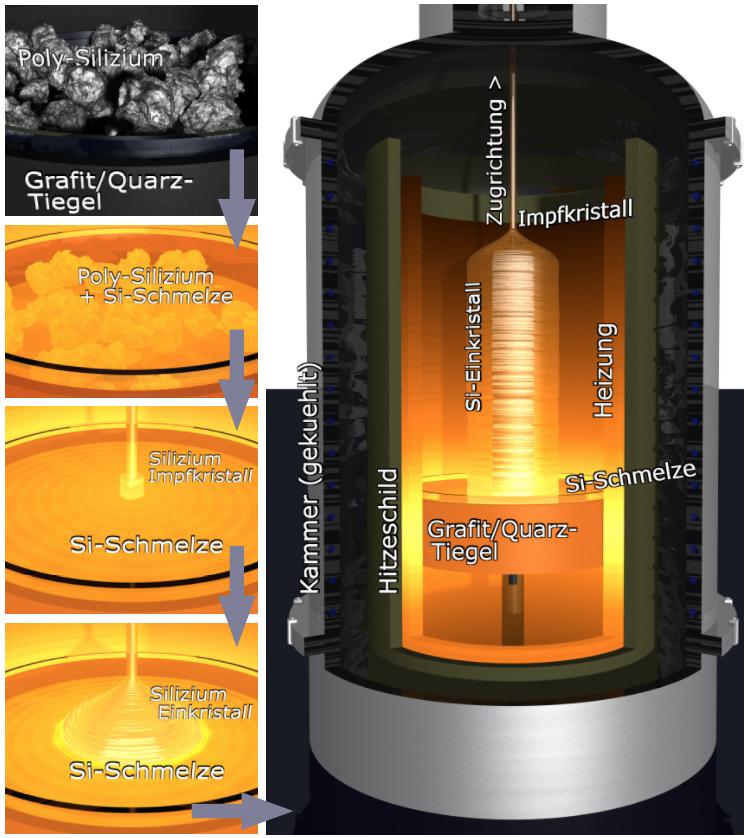
This stage transforms high-purity polysilicon into single-crystal silicon ingots, which are then sliced and polished into wafers.
Key equipment includes:
- Crystal growth furnaces
- Multi-wire saws
- Double-side grinding systems
- Chemical Mechanical Polishing tools
- Cleaning and inspection systems
This step determines wafer flatness, defect density, and overall substrate quality.
2.2 Oxidation
Oxidation forms a uniform silicon dioxide layer on the wafer surface, serving as an insulating or masking layer.
Core equipment:
- Oxidation/diffusion furnaces
- Rapid thermal processing (RTP) systems
- Ion implantation systems
- Wafer cleaning tools
2.3 Photolithography
Photolithography transfers circuit patterns from masks onto the wafer using light exposure.
Key equipment includes:
- Lithography systems (EUV/DUV)
- Photoresist coating and developing tracks
- Mask inspection tools
- Critical dimension (CD) measurement systems
This step defines the minimum feature size and process node.
2.4 Etching
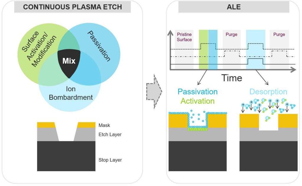
Etching removes unwanted material to transfer patterns into underlying layers.
Main equipment:
- Dry etching (plasma etching) systems
- Wet etching tools
- Endpoint detection systems
Advanced processes increasingly rely on Atomic Layer Etching for atomic-scale precision.
2.5 Thin Film Deposition
Thin film deposition builds functional layers such as dielectrics, metals, and semiconductors.
Major techniques include:
- Chemical Vapor Deposition
- Physical Vapor Deposition
- Atomic Layer Deposition
- Epitaxial growth
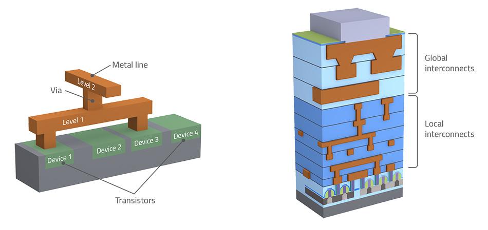
2.6 Metallization and Interconnect
7
This stage forms electrical connections between devices using metal layers.
Key equipment:
- Electroplating systems
- CMP tools
- Metal deposition systems
- Via and trench etching tools
2.7 Testing
6
Testing ensures functionality and filters defective chips.
Core equipment:
- Automated Test Equipment (ATE)
- Probe stations
- Sorting systems
- Inspection tools
2.8 Packaging
Packaging protects chips and enables electrical connections and heat dissipation.
Equipment includes:
- Die bonding systems
- Wire bonding tools
- Flip-chip bonding systems
- Molding and trimming tools
- Through-Silicon Via processing systems
3. Five Core Front-End Equipment Categories
Front-end equipment accounts for over 80% of total fab investment and represents the technological core of semiconductor manufacturing.
3.1 Lithography Systems
Lithography defines the smallest feature size and is often considered the most critical and complex equipment category.
Key characteristics:
- Ultra-high precision optics
- Nanometer-scale alignment
- Extreme system integration
3.2 Etching Systems
Etching systems transfer patterns into materials and are among the highest value contributors in fabrication.
Development trends:
- High anisotropy
- Atomic-level precision
- Multi-material compatibility
3.3 Deposition Systems
Deposition tools construct multilayer device structures.
Key advancements:
- Atomic-scale thickness control
- High uniformity
- Low defect density
3.4 Ion Implantation Systems
Ion implantation introduces dopants into the semiconductor lattice to control electrical properties.
Core capabilities:
- Precise energy and dose control
- Uniform implantation
- Broad energy range coverage
3.5 Metrology and Inspection Systems
Metrology tools provide process feedback and ensure yield control.
Functions include:
- Defect inspection
- Critical dimension measurement
- Thin film characterization
These systems are essential for advanced node manufacturing.
4. Technology Trends
The evolution of semiconductor equipment is driven by several key trends:
- Increasing precision approaching physical limits
- Higher levels of automation and system integration
- Growth of advanced packaging technologies
- Data-driven manufacturing and real-time process control
5. Conclusion
Semiconductor manufacturing equipment forms the backbone of the integrated circuit industry. Each fabrication step relies on specialized tools working in tightly controlled environments. As process nodes continue to shrink and application demands expand, equipment innovation remains the primary driver of technological progress.
Future advancements will focus on achieving higher precision, improved efficiency, and deeper integration across the manufacturing ecosystem, ensuring continued evolution of semiconductor technology.