
Semiconductor manufacturing equipment is widely regarded as the “industrial mother machine” of the integrated circuit (IC) industry, enabling the entire transformation from raw silicon materials to finished chips.
Among all segments of the semiconductor value chain, wafer fabrication equipment accounts for approximately 85% of total equipment investment, representing the highest technological barrier and the most capital-intensive domain.
Modern semiconductor fabs are no longer organized as simple linear production lines. Instead, they are designed as a multi-layered, modular, and loop-optimized system, structured around:
- Process flow–driven architecture
- Cleanliness-controlled zoning
- Automated material handling backbone
- Bottleneck-equipment-centered layout
The ultimate objectives of fab design include:
- Maximizing utilization of bottleneck tools
- Minimizing wafer transport distance and cycle time
- Strict contamination control
- Ensuring scalability and future node migration capability
This integrated system forms a highly complex yet efficient manufacturing ecosystem.
1. Overview of the Semiconductor Equipment Ecosystem
The semiconductor manufacturing equipment industry can be divided into six major segments:
1.1 Semiconductor Materials Preparation Equipment (Upstream)
This segment supports the production of raw semiconductor materials, forming the foundation of the entire supply chain.
Key processes include:
- Silicon crystal growth and wafer slicing
- Wafer polishing and surface conditioning
- Compound semiconductor material synthesis
Key technical challenges focus on:
- Ultra-high purity control
- Crystal defect minimization
- Diameter and thickness uniformity
1.2 Design Verification Equipment
Used during chip design and validation stages to ensure electrical and functional correctness before mass production.
Typical systems include:
- High-speed signal integrity testing platforms
- Device electrical characterization systems
- Timing and power analysis instruments
These tools ensure design feasibility and manufacturability.
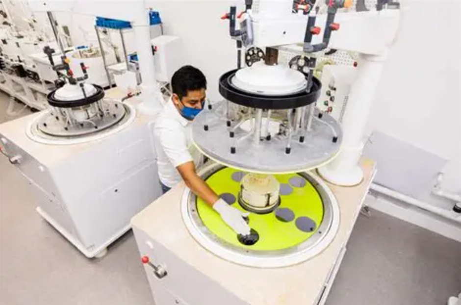
1.3 Wafer Fabrication Equipment (Core Segment)
This is the most critical and capital-intensive segment, directly determining semiconductor technology nodes.
Main categories include:
- Lithography systems
- Etching systems
- Thin film deposition systems
- Ion implantation and annealing systems
- Cleaning and metrology systems
This segment defines manufacturing capability for nodes such as 28nm, 7nm, and 3nm.
1.4 Semiconductor Packaging Equipment
Packaging transforms fabricated wafers into functional chips and establishes electrical connectivity.
Main categories:
- Traditional packaging equipment (wire bonding, etc.)
- Advanced packaging systems (flip-chip, 2.5D/3D integration)
Advanced packaging is becoming a key extension of Moore’s Law.
1.5 Semiconductor Testing Equipment
Used for final chip verification and quality assurance, including:
- Automated Test Equipment (ATE)
- Probe stations
- Sorting and binning systems
These systems ensure yield and reliability before shipment.
1.6 Semiconductor Inspection and Analytical Equipment
Used for process monitoring and failure analysis:
- Defect inspection systems
- Material composition and structural analysis tools
- Reliability testing platforms
They provide feedback for process optimization and yield improvement.
2. Modern Fab Layout Architecture
Modern semiconductor fabs are highly engineered environments with strict architectural logic.
2.1 Process Flow–Driven Layout
Wafer processing follows a strict sequential flow:
Material preparation → Lithography → Etching → Deposition → Doping → Thermal processing → Cleaning → Metrology
Equipment placement strictly follows this flow to prevent backtracking and contamination.
2.2 Cleanroom Zoning Strategy
Fabs are divided into multiple cleanliness levels:
- Ultra-clean zones (advanced lithography and etching)
- High-clean zones (deposition and implantation)
- Standard clean zones (support processes)
Airflow and personnel movement are strictly controlled in a unidirectional manner.
2.3 Automated Material Handling System (AMHS)
Wafer transport is fully automated to minimize human contact:
- Overhead hoist transport systems (OHT)
- Automated guided vehicles (AGV)
- Automated storage and retrieval systems (AS/RS)
The goal is to ensure zero contamination risk and high throughput efficiency.
2.4 Bottleneck-Centered Layout Design
Critical equipment (such as advanced lithography tools) typically defines fab throughput.
Key principles include:
- Layout centered around bottleneck tools
- Symmetrical upstream/downstream optimization
- Maximization of tool utilization rate
2.5 Modular and Scalable Fab Design
Fabs are constructed in modular cleanroom blocks to enable:
- Capacity expansion
- Technology node upgrades
- Multi-node coexistence
This ensures long-term flexibility and cost efficiency.
3. Core Semiconductor Equipment Technologies
3.1 Lithography Systems
Lithography is the most critical step in semiconductor manufacturing, responsible for transferring circuit patterns onto wafers.
Technology classifications include:
- Extreme Ultraviolet (EUV) lithography for 7nm and below
- ArF immersion lithography for 28nm–7nm nodes
- Dry ArF lithography for mature nodes
- i-line lithography for legacy processes
EUV systems are among the most complex industrial machines ever built, integrating:
- High-energy EUV light sources (13.5nm wavelength)
- Multi-layer reflective optical systems
- Nanometer-precision dual-stage wafer positioning
- High-vacuum environments
3.2 Etching Systems
Etching equipment removes material selectively to form transistor structures.
Main types include:
- Capacitive Coupled Plasma (CCP) etching
- Inductively Coupled Plasma (ICP) etching
- Deep Reactive Ion Etching (DRIE)
- Atomic Layer Etching (ALE)
Key trends:
- Atomic-scale precision control
- High aspect ratio structure capability
- Improved selectivity and uniformity
3.3 Thin Film Deposition Systems
Used to deposit functional layers on wafers:
- Plasma-Enhanced Chemical Vapor Deposition (PECVD)
- Low-Pressure Chemical Vapor Deposition (LPCVD)
- High-Density Plasma CVD (HDPCVD)
- Physical Vapor Deposition (PVD)
- Atomic Layer Deposition (ALD)
ALD enables atomic-level thickness control with near-perfect conformality.
3.4 Ion Implantation and Thermal Processing
These systems modify the electrical properties of semiconductors:
- Ion implantation introduces dopants with precise energy control
- Rapid Thermal Annealing (RTA) activates dopants and repairs crystal damage
- Laser annealing enables ultra-fast localized heating for advanced nodes
Key requirements include:
- Precise dose and energy control
- High uniformity
- Minimal thermal budget impact
3.5 Cleaning and Metrology Systems
Cleaning systems are used throughout all process steps to remove:
- Particle contamination
- Organic residues
- Metallic impurities
Metrology systems provide real-time process control by measuring:
- Critical dimension (CD)
- Film thickness
- Overlay accuracy
- Defect density
4. Technology Development Trends
4.1 Transition Toward Atomic-Scale Manufacturing
Semiconductor manufacturing is approaching physical limits, requiring:
- Atomic layer-level process control
- Ultra-low defect density
- Sub-nanometer precision
4.2 Multi-Physics Process Integration
Future equipment integrates:
- Optical systems
- Plasma physics
- Thermal dynamics
- Electromagnetic control
for highly synchronized process execution.
4.3 AI-Driven Manufacturing Intelligence
Artificial intelligence is increasingly used for:
- Process optimization
- Predictive maintenance
- Real-time yield improvement
4.4 Advanced Packaging and System Integration
As Moore’s Law slows, innovation shifts toward:
- 3D heterogeneous integration
- Chiplet architectures
- System-level packaging (SiP, 2.5D/3D stacking)
Conclusion
Semiconductor manufacturing equipment represents one of the most advanced and complex industrial systems ever developed. It integrates precision engineering, materials science, plasma physics, optics, automation, and data intelligence into a unified manufacturing ecosystem.
Each tool within a semiconductor fab is not an isolated machine but part of a highly synchronized and interdependent process network.
As semiconductor nodes continue to scale toward physical limits, equipment complexity, precision, and integration will continue to increase—making this industry a cornerstone of global technological competition.