


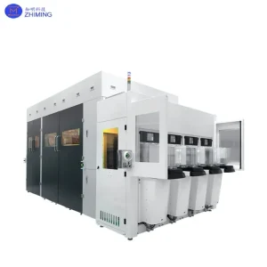
The Wafer Bonding Equipment is a high-performance system engineered for advanced semiconductor packaging, MEMS fabrication, and third-generation semiconductor integration. It supports 2-inch to 12-inch wafers and enables room-temperature direct bonding and hydrophilic bonding, making it particularly suitable for Si-Si, SiC-SiC, and heterogeneous material bonding (Si-SiC, GaN, Sapphire, etc.).
Designed for both R&D environments and mass production, the system integrates ultra-precision alignment, closed-loop pressure and temperature control, and ultra-high vacuum bonding conditions, ensuring high bonding strength, excellent interface uniformity, and low defect density.
Caractéristiques principales
 1. Advanced Room-Temperature Bonding Technology
- Eliminates thermal stress and wafer warpage
- Enables bonding of temperature-sensitive and dissimilar materials
- Supports hydrophilic bonding and plasma-activated bonding
2. Ultra-High Precision Alignment
- Mark alignment accuracy: ≤ ±2 μm
- Edge alignment accuracy: ≤ ±50 μm
- Optional upgrade to submicron alignment system
3. High Bonding Strength & Interface Quality
- ≥ 2.0 J/m² (Si-Si direct bonding at room temperature)
- Up to ≥5 J/m² with plasma surface activation
- Excellent interface cleanliness under UHV conditions
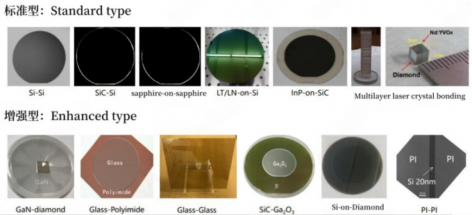
4. Wide Material Compatibility
Supports bonding of:
- Semiconductors: Si, SiC, GaN, GaAs, InP
- Optical materials: Sapphire, Glass
- Functional materials: LiNbO₃, Diamond
5. Flexible Process Capability
- Wafer size: 2″ – 12″
- Compatible with irregular-shaped samples
- Optional modules: pre-heating / annealing (RT–500°C)
Spécifications techniques
| Paramètres | Spécifications |
|---|---|
| Bonding Methods | Direct Bonding / Plasma-Activated Bonding |
| Taille de la plaquette | 2″ – 12″ |
| Gamme de pression | 0 – 10 MPa |
| Max Force | 100 kN |
| Plage de température | Room Temp – 500°C (Optional) |
| Niveau de vide | ≤ 5 × 10⁻⁶ Torr |
| Alignment Accuracy | ≤ ±2 μm (Mark), ≤ ±50 μm (Edge) |
| Bonding Strength | ≥ 2.0 J/m² (RT Si-Si) |
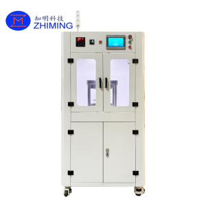
 Système de contrôle intelligent
- Industrial-grade touchscreen HMI
- Supports 50+ process recipes storage
- Real-time pressure-temperature closed-loop control
- Stable and repeatable process performance
Safety & Reliability
- Triple interlock protection (pressure / temperature / vacuum)
- Emergency stop system
- Designed for Class 100 cleanroom compatibility
Configurations optionnelles
- Robotic wafer handling system
- SECS/GEM communication interface (fab integration ready)
- Inline inspection module
- Plasma surface activation unit
Applications typiques
1. MEMS Packaging
Hermetic sealing for sensors such as accelerometers and gyroscopes
2. 3D IC Integration
Wafer stacking for TSV and advanced packaging
3. Compound Semiconductor Devices
GaN / SiC power device bonding and layer transfer
4. CMOS Image Sensors (CIS)
Low-temperature bonding of CMOS wafers and optical substrates
5. Biochips & Microfluidics
Reliable bonding for lab-on-chip devices
Process Example
LiNbO₃ – SiC Wafer Bonding (Room Temperature)
- Achieves strong and uniform bonding interface
- Verified by cross-sectional TEM imaging
- Suitable for high-frequency and optoelectronic applications
Q&A
Q1: Why choose room-temperature wafer bonding instead of thermal bonding?
Room-temperature bonding avoids thermal mismatch and stress, making it ideal for heterogeneous materials and improving yield in advanced packaging.
Q2: What materials can be bonded?
The system supports a wide range of materials including:
- Semiconductors: Si, SiC, GaN
- Oxides: SiO₂, LiNbO₃
- Metals: Cu, Au
Why Choose This System
- Proven performance in SiC power device manufacturing
- Verified bonding strength through lab testing and TEM analysis
- Designed for both research institutes and industrial fabs
- Modular architecture ensures long-term scalability and upgradeability
Avis
Il n’y a pas encore d’avis.