
1. Introduction: Why Wafer Thinning Matters
In modern semiconductor manufacturing, the transition from front-end processing to back-end packaging begins with two critical steps: back grinding (wafer thinning) and polishing.
After wafers complete front-end fabrication and electrical testing, they must undergo controlled thinning to meet increasingly demanding requirements in:
- Advanced packaging
- Thermal management
- Device miniaturization
- High-frequency performance
Wafer thickness is no longer just a structural parameter—it directly impacts chip performance, yield, reliability, and cost efficiency.
2. Core Objectives of Wafer Back Grinding and Polishing
2.1 Enhanced Thermal Performance
Thinner wafers improve heat dissipation by reducing the thermal path. This is especially critical in:
- Power devices (Si, SiC)
- High-density ICs
- RF applications
Efficient heat removal prevents overheating and extends device lifespan.
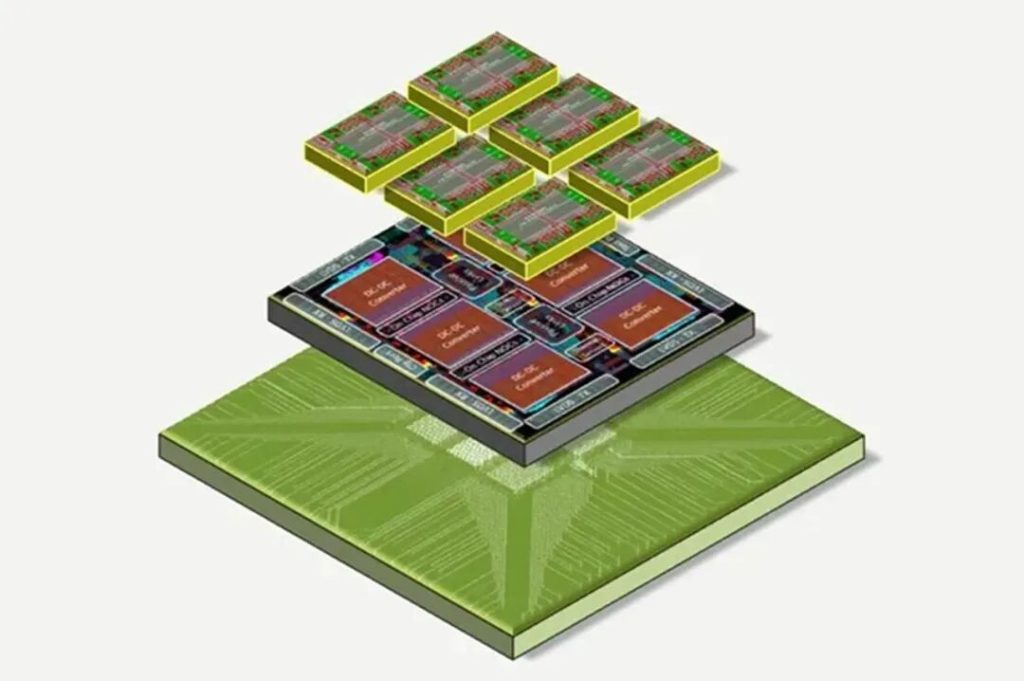
2.2 Compatibility with Advanced Packaging
Modern packaging technologies—such as:
- 3D stacking (Stacking)
- System-in-Package (SiP)
- Flip-chip
—require ultra-thin wafers (often below 100 μm).
Thinning enables:
- Smaller form factors
- Reduced package weight
- Higher integration density
2.3 Improved Mechanical Flexibility
Thinner wafers exhibit greater flexibility, enabling applications in:
- Wearable electronics
- Flexible devices
- Advanced sensors
2.4 Electrical Performance Optimization
Wafer thinning reduces parasitic capacitance, which is critical in:
- High-frequency circuits
- RF and microwave devices
This leads to improved signal integrity and device efficiency.
2.5 Yield Improvement
Polishing removes:
- Surface defects
- Residual stress layers
- Micro-cracks from grinding
This significantly enhances final chip yield and reliability.
3. Standard Wafer Thinning Process Flow
A typical back grinding and polishing process consists of four key steps:
Step 1: Temporary Bonding
- Wafer is attached to a carrier using:
- Adhesive tape (tape lamination)
- Wax bonding to glass/ceramic substrates
This protects the front side during thinning.
Step 2: Back Grinding (Material Removal)
- Mechanical or chemical methods are used to remove bulk material.
- This is the primary thickness reduction stage.
Step 3: Polishing
- Removes:
- Grinding marks
- Subsurface damage
- Residual stress
Ensures a smooth, defect-free surface.
Step 4: Debonding
- Wafer is separated from the carrier via:
- UV exposure
- Chemical dissolution
4. Four Main Wafer Thinning Technologies
4.1 Mechanical Grinding
Principle:
Material removal via diamond grinding wheels.
Avantajlar:
- High efficiency
- Suitable for bulk removal
Limitations:
- Surface damage layer
- Mikro çatlaklar
- Requires polishing follow-up
4.2 Lapping (Mechanical Polishing)
Principle:
Abrasive particles roll and micro-cut the surface.
Characteristics:
- Produces matte, uniform surfaces
- Less aggressive than grinding
Best for:
- Controlled thinning
- Intermediate finishing
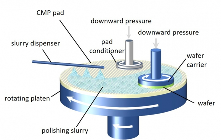
4.3 Chemical Mechanical Polishing (CMP)
Principle:
Combines:
- Chemical reaction (surface softening)
- Mechanical removal
Avantajlar:
- उत्कृष्ट surface flatness
- Nanometer-level roughness
- Global planarization
Limitations:
- Higher cost
- Complex process control
4.4 Wet & Dry Etching
Wet Etching
- Uses chemical solutions
- Low cost, simple setup
- Poor uniformity control
Dry Etching
- Uses plasma-based reactions
- High precision (in theory)
- Expensive and complex
Conclusion:
Etching is rarely used as a primary thinning method for high-precision wafers.
5. Process Comparison Summary
| Method | Efficiency | Surface Quality | Cost | Typical Use |
|---|---|---|---|---|
| Grinding | High | Low | Medium | Bulk removal |
| Lapping | Medium | Medium | Medium | Intermediate |
| CMP | Low | Very High | High | Final polishing |
| Etching | Low | Low | Variable | Special cases |
6. Key Challenges in Wafer Thinning
6.1 Thickness Uniformity (TTV Control)
Maintaining low Total Thickness Variation (TTV) is critical for device consistency.
6.2 Surface Defect Control
Common issues include:
- Scratches
- Mikro çatlaklar
- Particle contamination
6.3 Stress Management
Mechanical and thermal stresses can cause:
- Warpage
- Cracking
- Device failure
7. How to Improve Wafer Thinning Quality
7.1 Optimize Consumables
- Match abrasive size to material hardness
- Use multi-stage grit reduction
7.2 Fine-Tune Equipment Parameters
Key parameters:
- Downforce pressure
- Rotation speed
- Feed rate
7.3 Introduce Polishing Steps
Post-grinding polishing:
- Removes damage layer
- Reduces stress
- Improves surface roughness
8. Equipment Capability and Process Results
Typical industry-level performance:
- Wafer size: up to 6-inch (compatible with smaller samples)
- Minimum sample size: 1 cm × 1 cm
- Materials supported:
- Silicon (Si)
- Gallium Arsenide (GaAs)
- Indium Phosphide (InP)
Process Accuracy
- 4-inch wafer TTV: ±3 μm
- 6-inch wafer TTV: ±5 μm
Surface Quality
- Surface roughness: Ra ≤ 0.5 nm (@1 μm²)
Final Thickness
- Standard wafers: ~100 μm
- Bonded wafers: ~50 μm
9. Industry Insight: The Balance Between Thickness and Performance
As semiconductor devices evolve toward:
- Higher integration
- 3D stacking
- Advanced packaging
Wafer thinning becomes a strategic process step, not just a mechanical operation.
However, an important trade-off exists:
Thinner wafers enable higher integration—but excessive thinning may degrade mechanical stability and device performance.
Therefore, selecting the right thinning method and process window is essential for:
- Cost control
- Yield optimization
- Long-term reliability
10. Sonuç
Wafer back grinding and polishing are foundational technologies bridging front-end fabrication and advanced packaging.
A well-optimized thinning process can:
- Improve thermal and electrical performance
- Enable advanced packaging architectures
- Increase yield and reduce costs
As semiconductor technology advances, precision, stability, and process integration in wafer thinning will continue to define competitive advantage.