
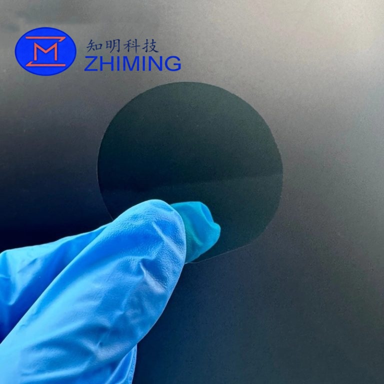


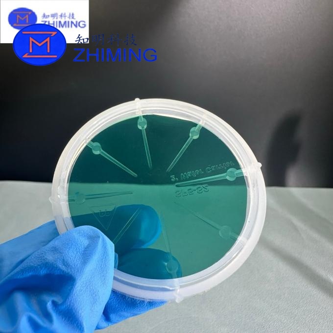
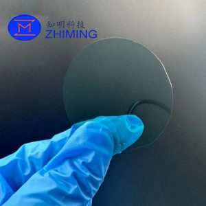
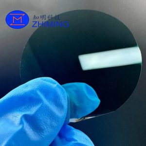
 The 2-inch 6H-N Silicon Carbide wafer is a single crystal substrate engineered for both research and device-level applications. The 6H polytype features a hexagonal crystal structure that provides stable electrical conductivity and good thermal performance under demanding conditions.
With a bandgap of approximately 3.02 eV, 6H-SiC enables operation in environments where traditional silicon materials fail, particularly in high-voltage, high-temperature, and high-frequency conditions. This makes it suitable for early-stage device prototyping, material testing, and specialized electronic component fabrication.
ZMSH SiC wafers are manufactured using controlled crystal growth techniques to ensure consistent resistivity, low defect density, and high surface quality. These parameters are critical for ensuring reproducible experimental results and stable device performance.
Key Features
N-Type Conductive Structure
The wafer is doped as N-type, providing stable electron conduction pathways suitable for semiconductor device fabrication and electrical characterization experiments.
Wide Bandgap Semiconductor Material
With a bandgap of ~3.02 eV, SiC supports significantly higher electric field strength compared to silicon, enabling high-voltage operation and improved device efficiency.
High Thermal Conductivity
SiC exhibits excellent thermal conductivity, allowing efficient heat dissipation from active device regions. This improves device reliability and extends operational lifetime in high-power applications.
High Mechanical Strength
With a Mohs hardness of approximately 9.2, SiC wafers offer strong resistance to mechanical damage, surface wear, and processing stress during fabrication.
High Breakdown Electric Field
The high breakdown field strength enables compact device structures while maintaining high voltage tolerance, making SiC ideal for advanced power electronics.
Technical Specifications
| Parameter | Specification |
|---|---|
| Material | Single Crystal Silicon Carbide |
| Brand | ZMSH |
| Polytype | 6H-N |
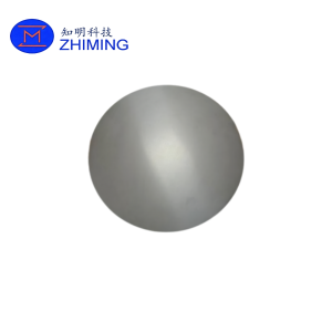
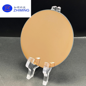
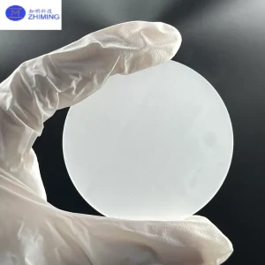
| Diameter | 2 inch (50.8 mm) |
| Thickness | 350 μm / 650 μm |
| Conductivity Type | N-type |
| Surface Finish | CMP Polished Si-face |
| C-face Treatment | Mechanical Polished |
| Surface Roughness | Ra < 0.2 nm (Si-face) |
| Resistivity | 0.015 – 0.028 Ω·cm |
| Color | Transparent / Light Green |
| Packaging | Single Wafer Container |
Material Properties of 6H-SiC
| Property | Value |
|---|---|
| Lattice Parameters | a = 3.073 Å, c = 15.117 Å |
| Mohs Hardness | ≈ 9.2 |
| Density | 3.21 g/cm³ |
| Thermal Expansion Coefficient | 4–5 ×10⁻⁶ /K |
| Refractive Index (750 nm) | n₀ = 2.60, nₑ = 2.65 |
| Dielectric Constant | ≈ 9.66 |
| Thermal Conductivity | ~3.7–3.9 W/cm·K |
| Bandgap | 3.02 eV |
| Breakdown Electric Field | 3–5 ×10⁶ V/cm |
| Saturation Drift Velocity | 2.0 ×10⁵ m/s |
These intrinsic physical properties make 6H-SiC suitable for applications requiring stable performance in extreme electrical and thermal conditions.
 Manufacturing Process
SiC single crystal wafers are typically produced using the Physical Vapor Transport (PVT) method, a mature industrial process for wide bandgap semiconductor crystal growth.
In this process, high-purity SiC source material is sublimated at temperatures above 2000°C. The vapor species are transported through a carefully controlled thermal gradient and recrystallized on a seed crystal, forming a single crystal ingot (boule). After growth, the boule is processed into wafers through slicing, lapping, polishing, and cleaning steps.
For device applications, wafers can undergo additional Chemical Vapor Deposition (CVD) epitaxial growth, which allows precise control of doping concentration and layer thickness. This step is essential for MOSFET and diode fabrication.
Applications
Power Electronics
2-inch 6H-N SiC wafers are used in the development and prototyping of power semiconductor devices, including diodes, MOSFET structures, and power modules. These devices are essential for energy conversion systems and power management circuits.
High-Temperature Electronics
SiC materials maintain stable electrical performance at elevated temperatures, making them suitable for aerospace electronics, industrial monitoring systems, and energy infrastructure applications.
Semiconductor Research and Development
Due to their availability and cost-effectiveness, 2-inch wafers are widely used in university laboratories, research institutes, and pilot production environments for material studies and device experimentation.
Optoelectronic and Special Applications
SiC also exhibits optical transparency in certain wavelength ranges, allowing its use in specialized photonic and optoelectronic research applications.
Advantages
The 2-inch SiC wafer platform provides several advantages for research and development:
- Lower cost compared to larger wafer sizes
- Easier handling for laboratory-scale experiments
- Suitable for rapid prototyping and process testing
- Stable crystal quality for reproducible results
- Flexible customization options for research needs
FAQ
Q1: What is the difference between 6H-SiC and 4H-SiC?
6H-SiC and 4H-SiC are different crystal polytypes. 4H-SiC generally offers higher electron mobility and is widely used in commercial power devices, while 6H-SiC provides stable electrical behavior and is commonly used in research and specific electronic applications.
Q2: What surface treatment is applied to the wafer?
The Si-face is polished using chemical mechanical polishing (CMP) to achieve ultra-smooth surface quality (Ra < 0.2 nm). The C-face is mechanically polished to support different processing requirements.
Q3: Can wafer specifications be customized?
Yes. ZMSH provides customization options including thickness, doping concentration, resistivity range, and surface preparation according to customer requirements.
Reviews
There are no reviews yet.