


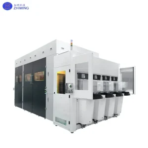
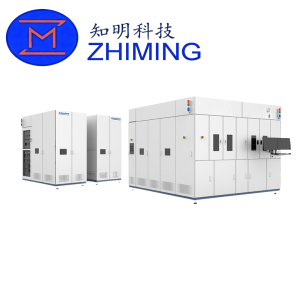
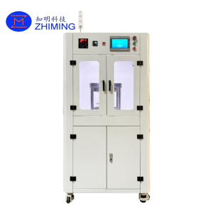
 The Semi Automatic Room Temperature Wafer Bonding Machine is a high-precision system for wafer-level and chip-level bonding. By combining mechanical pressure with in situ surface activation technology, it enables permanent bonding at room temperature (20–30°C) without adhesives or high temperature processing. This minimizes thermal stress and material deformation, making it ideal for heat-sensitive and heterogeneous materials. The machine supports wafer sizes from 2 inch to 12 inch and is suitable for research, pilot production, and small to medium scale manufacturing.
 Key Features
- Room Temperature Bonding – Operates at 25 ± 5°C to prevent thermal mismatch and wafer warpage.
- Surface Activation – Plasma or chemical activation improves bonding strength; optional sputtering enhances interface quality.
- High Precision Alignment – Visual alignment system and precision motion platform with ±0.5 μm accuracy.
- Wide Material Compatibility – Supports Si, SiC, GaAs, GaN, InP, sapphire, glass, LiNbO₃, LiTaO₃, diamond, and selected polymers.
- Semi-Automatic Operation – Manual wafer loading with automated bonding process; programmable recipes for repeatable results.
- Clean and Stable Environment – Built-in Class 100 clean system ensures low contamination and interface void rate <0.1%.
Technical Specifications
| Parameter | Specification |
|---|---|
| Wafer Size | 2″ – 12″, compatible with irregular samples |
| Bonding Temperature | 20–30°C |
| Maximum Pressure | 80 kN |
| Pressure Control | 0–5000 N adjustable, ±1 N resolution |
| Alignment Accuracy | ±0.5 μm |
| Bond Strength | ≥2.0 J/m² |
| Surface Treatment | In situ activation + sputtering deposition |
| Feeding Mode | Manual |
| Cleanliness Level | Class 100 |
Core Technology
- Room Temperature Direct Bonding – Activated surfaces contact under controlled pressure forming stable bonds without thermal annealing.
- Surface Activation – Increases surface energy, removes contaminants, and improves bonding uniformity across materials.
 Applications
- Advanced Semiconductor Packaging – 3D IC stacking, TSV bonding, heterogeneous integration of logic and memory chips.
- MEMS Manufacturing – Wafer-level vacuum packaging for sensors such as accelerometers and gyroscopes.
- Optoelectronics and Displays – LED bonding, sapphire and glass substrate bonding, AR/VR optical module assembly.
- Microfluidics and Biochips – PDMS and glass bonding while preserving biological activity.
- Research and Emerging Devices – Flexible electronics, quantum devices, and heterogeneous material integration.
Service and Support
- Process Development – Bonding parameter optimization and surface activation solutions for different materials.
- Equipment Customization – High-precision alignment modules, vacuum or controlled atmosphere chambers.
- Technical Training – On-site operation guidance and process debugging.
- After-Sales Support – 12-month warranty, quick replacement of key components, remote diagnostics, and software updates.
FAQ
Q: What is the main advantage of room temperature bonding?
A: It eliminates thermal stress and enables reliable bonding of heat-sensitive and heterogeneous materials.
Q: What materials can be bonded?
A: Silicon, silicon carbide, gallium nitride, gallium arsenide, indium phosphide, sapphire, glass, lithium niobate, diamond, and selected polymers.

Reviews
There are no reviews yet.