
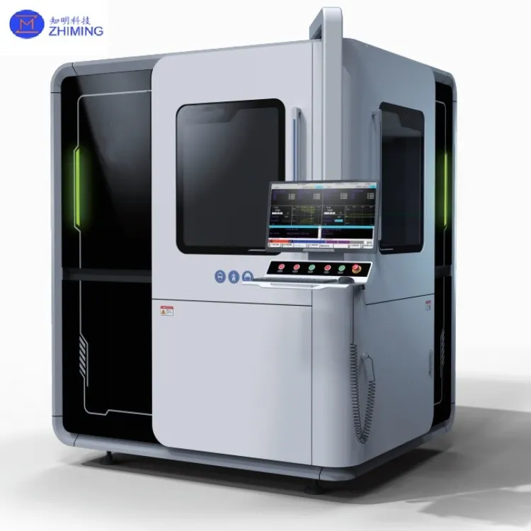
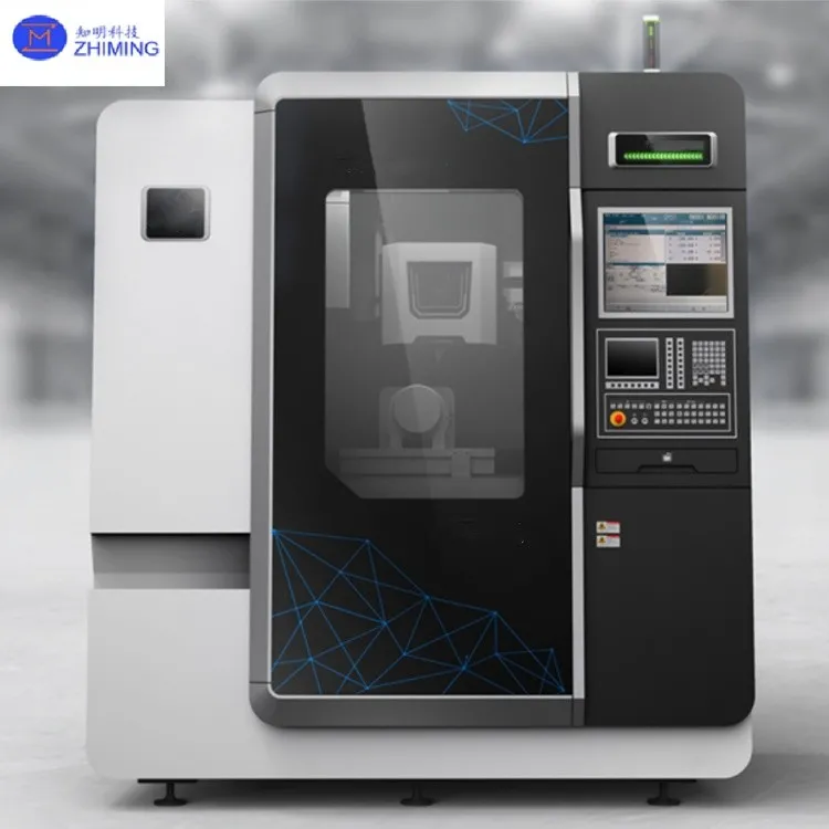
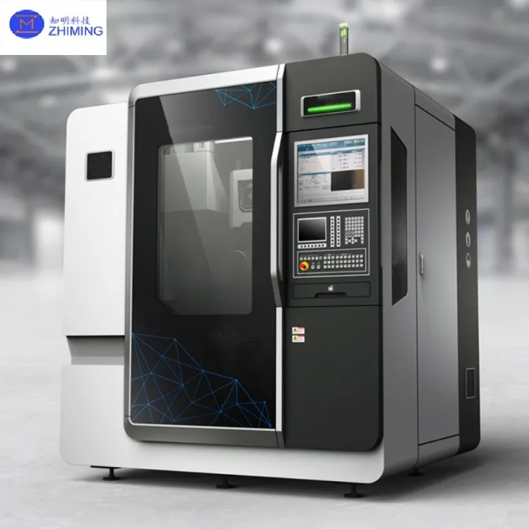
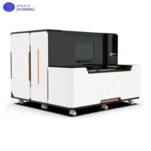
 Thiết bị laser vi lưu sử dụng công nghệ laser tia nước vi mô tiên tiến để mang lại khả năng gia công với độ chính xác cao và ít gây hư hại nhiệt cho các tấm bán dẫn cũng như các vật liệu cứng, giòn hoặc có khoảng cách dải năng lượng rộng. Bằng cách kết hợp tia nước có kích thước dưới micromet với chùm tia laser, hệ thống hướng năng lượng laser chính xác đến bề mặt vật liệu gia công, trong khi dòng nước liên tục làm mát và loại bỏ các mảnh vụn. Công nghệ này giải quyết hiệu quả các thách thức phổ biến của gia công laser và cơ học truyền thống, bao gồm tổn thương nhiệt, vết nứt vi mô, nhiễm bẩn, độ dốc và biến dạng.
 Các tính năng chính
- Loại laser: Laser Nd:YAG trạng thái rắn bơm bằng điốt, bước sóng 532/1064 nm, độ rộng xung tính bằng μs/ns, công suất trung bình 10–200 W
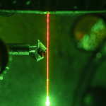
- Hệ thống phun nước áp lực cao: Nước lọc, khử ion, áp suất thấp; vòi phun siêu mịn chỉ tiêu thụ 1 lít/giờ ở áp suất 300 bar, lực tác động không đáng kể (<0,1 N)
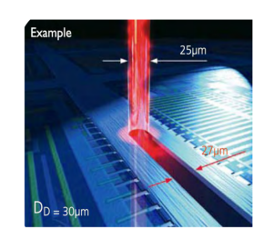
- Đầu phun: Ngọc bích hoặc kim cương, đường kính 30–150 μm để định hướng laser chính xác
- Hệ thống phụ trợ: Bơm áp suất cao và các thiết bị xử lý nước đảm bảo hiệu suất phun ổn định
- Độ chính xác: Độ chính xác định vị ±5 μm, độ chính xác định vị lặp lại ±2 μm
- Khả năng xử lý: Độ nhám bề mặt Ra ≤ 1,2–1,6 μm, tốc độ cắt tuyến tính ≥ 50 mm/s, tốc độ mở ≥ 1,25 mm/s, tốc độ cắt theo chu vi ≥ 6 mm/s
Thông số kỹ thuật
| Thông số kỹ thuật | Lựa chọn 1 | Lựa chọn 2 |
|---|---|---|
| Thể tích mặt bàn (mm) | 300 × 300 × 150 | 400 × 400 × 200 |
| Trục tuyến tính XY | Động cơ tuyến tính | Động cơ tuyến tính |
| Trục tuyến tính Z | 150 | 200 |
| Độ chính xác định vị (μm) | ±5 | ±5 |
| Độ chính xác định vị lặp lại (μm) | ±2 | ±2 |
| Lực gia tốc (G) | 1 | 0.29 |
| Điều khiển số | 3 trục / 3+1 trục / 3+2 trục | 3 trục / 3+1 trục / 3+2 trục |
| Bước sóng (nm) | 532/1064 | 532/1064 |
| Công suất định mức (W) | 50/100/200 | 50/100/200 |
| Áp suất tia nước (bar) | 50–100 | 50–600 |
| Kích thước vòi phun (μm) | 30–150 | 30–150 |
| Kích thước máy (mm) | 1445×1944×2260 | 1700 × 1500 × 2120 |
| Trọng lượng (T) | 2.5 | 3 |
Ứng dụng
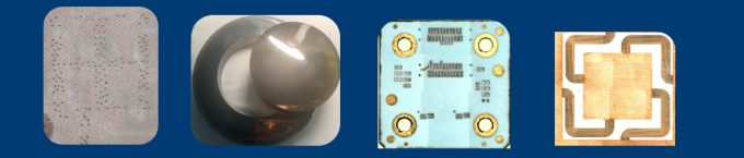
- Cắt và chia miếng wafer
- Vật liệu: Silic (Si), cacbua silic (SiC), nitrua gali (GaN) và các tấm wafer cứng/dễ vỡ khác
- Ưu điểm: Thay thế các lưỡi cắt kim cương truyền thống, giảm hiện tượng gãy mép (20 μm), tăng tốc độ cắt lên 30%, cho phép cắt ẩn đối với các tấm wafer siêu mỏng (<50 μm)
- Khoan chip và gia công lỗ siêu nhỏ
- Ứng dụng: Khoan lỗ xuyên silicon (TSV), mảng lỗ vi mô tản nhiệt cho các thiết bị công suất
- Đặc điểm: Đường kính lỗ 10–200 μm, tỷ lệ chiều sâu trên chiều rộng lên đến 10:1, độ nhám bề mặt Ra <0,5 μm
- Công nghệ đóng gói tiên tiến
- Ứng dụng: Cổng kết nối RDL, đóng gói cấp wafer (Fan-Out WLP)
- Lợi ích: Giảm thiểu tác động cơ học, nâng cao năng suất lên trên 99,51%
- Công nghệ chế tạo chất bán dẫn hợp chất
- Vật liệu: GaN, SiC và các chất bán dẫn khe năng lượng rộng khác
- Các tính năng: Khắc rãnh cổng, ủ bằng laser, kiểm soát năng lượng chính xác để ngăn ngừa sự phân hủy nhiệt
- Sửa chữa lỗi và tinh chỉnh
- Ứng dụng: Hàn laser cho mạch bộ nhớ, điều chỉnh mảng thấu kính vi mô cho cảm biến quang học
- Độ chính xác: Kiểm soát năng lượng ±1%, sai số định vị khi sửa chữa <0,1 μm
Điểm nổi bật & Ưu điểm
- Quy trình xử lý ở nhiệt độ thấp, trong môi trường sạch sẽ và được kiểm soát chặt chẽ giúp giảm thiểu tối đa tổn thương do nhiệt, các vết nứt nhỏ và hiện tượng thu hẹp
- Tia nước siêu mịn đảm bảo hướng dẫn laser chính xác và loại bỏ mảnh vụn hiệu quả
- Thích hợp cho các vật liệu cứng, giòn và trong suốt như SiC, GaN, kim cương, LTCC và tinh thể quang điện
- Tương thích với quy trình sản xuất bán dẫn có độ chính xác cao, đóng gói tiên tiến, linh kiện hàng không vũ trụ và vi điện tử
- Tăng năng suất, giảm lãng phí nguyên liệu và duy trì các tính chất của nguyên liệu
Chứng nhận & Tuân thủ
- Tuân thủ RoHS
- Được thiết kế dành cho các ứng dụng bán dẫn đòi hỏi độ chính xác cao
- Hỗ trợ quy trình xử lý có thể tái tạo, lặp lại và tự động hóa
Câu hỏi thường gặp
1. Có thể gia công những loại vật liệu nào bằng thiết bị laser vi lưu?
Công nghệ laser vi lưu có thể gia công chính xác các vật liệu bán dẫn cứng, giòn và có khoảng cách dải năng lượng rộng, bao gồm silicon (Si), cacbua silic (SiC), nitrua gali (GaN), kim cương, đế gốm carbon LTCC, tinh thể quang điện và các vật liệu tiên tiến khác. Công nghệ này rất lý tưởng cho các ứng dụng yêu cầu mức độ hư hỏng do nhiệt tối thiểu và chất lượng bề mặt cao.
2. Công nghệ laser tia siêu nhỏ giúp cải thiện quy trình sản xuất tấm bán dẫn như thế nào?
Bằng cách kết hợp tia nước có độ chính xác dưới micromet với chùm tia laser, công nghệ này đạt được độ chính xác dưới micromet đồng thời giảm thiểu vùng chịu ảnh hưởng nhiệt, ô nhiễm và hiện tượng gãy mép. Công nghệ này thay thế các lưỡi dao cơ học truyền thống trong các quy trình cắt lát, khoan và tạo cấu trúc vi mô, từ đó nâng cao hiệu suất và giảm thiểu lãng phí vật liệu.
3. Thiết bị laser vi lưu chất phù hợp nhất với những ứng dụng nào?
Thiết bị này được sử dụng rộng rãi trong:
- Cắt miếng wafer và cắt miếng wafer siêu mỏng (<50 μm) theo phương pháp "stealth"
- Kỹ thuật khoan lỗ xuyên silicon (TSV) và mảng lỗ siêu nhỏ cho mạch tích hợp 3D và thiết bị công suất
- Các công nghệ đóng gói tiên tiến, chẳng hạn như mở cửa sổ RDL, đóng gói cấp tấm wafer (Fan-Out WLP) và quá trình khắc cổng/nung bằng laser cho các chất bán dẫn GaN và SiC

Đánh giá
Chưa có đánh giá nào.