
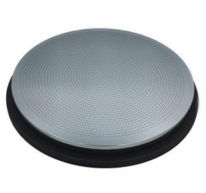
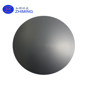
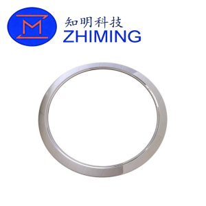
 シリコン電極は、エッチング装置、成膜装置、表面改質装置など、最先端の半導体プラズマ処理装置で使用される中核的な機能部品です。高純度単結晶シリコンから製造され、安定したプラズマ生成、均一な電界分布、正確なウェハー処理を保証する上で重要な役割を果たします。.
現代の半導体製造において、プロセスの安定性と歩留まりは、チャンバー内部部品の性能に直接影響されます。シリコン電極は、シリコンベースのプロセスとの優れた適合性により、汚染リスクを最小限に抑え、高いプロセス純度を維持することができるため、広く好まれています。金属電極と比較して、シリコン材料はプラズマによる汚染に対して優れた耐性を示し、より安定した電気特性を提供します。.
これらの電極は通常、高エネルギープラズマ、CFN_2084、SFN_2086、Cl_20などの反応性ガス、高温を伴う過酷な環境で使用されます。時間の経過とともに徐々に侵食されるため、次のように分類されます。 重要半導体消耗品, ライフサイクルを通じて高い性能を維持しながら、定期的な交換を必要とする。.
主な特徴
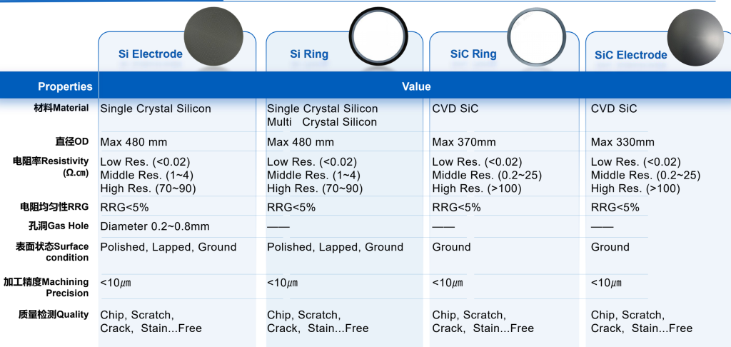
- 高純度素材:半導体グレードの単結晶シリコンを使用し、不純物を最小限に抑え、安定した電気性能を確保
- 複数の抵抗率オプション:低、中、高比抵抗グレードがあり、プラズマ制御の要求に応じて選択できる。
- 優れたプラズマ適合性:パーティクルの発生を抑え、ウェーハの歩留まりを向上
- 精密機械加工:ハイエンド半導体装置統合のための厳しい公差(<10μm)
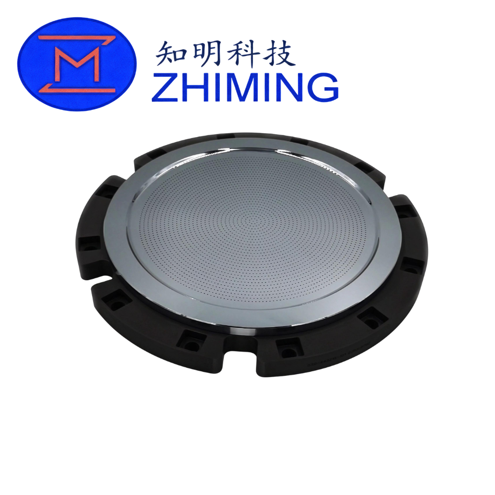
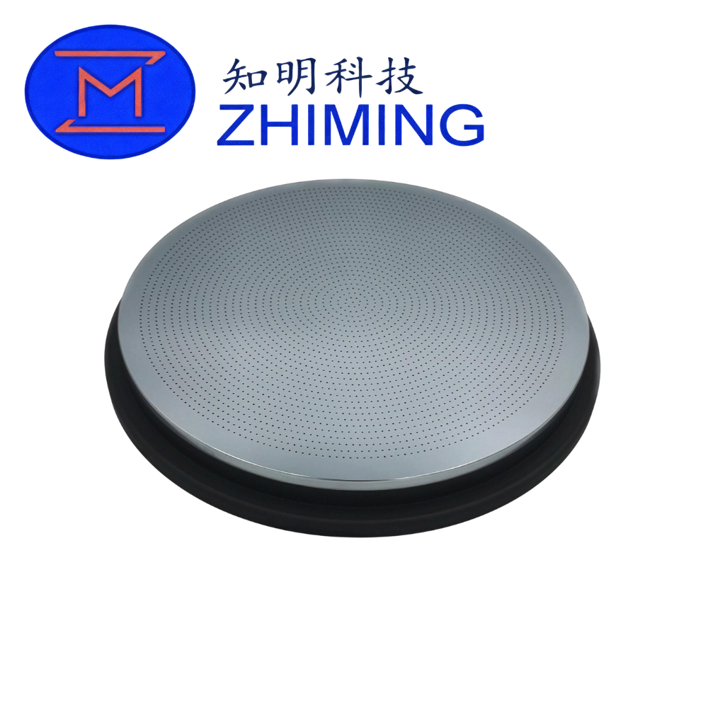
- カスタム・ガスホールデザイン:均一なガス分布とプラズマ密度の最適化に対応
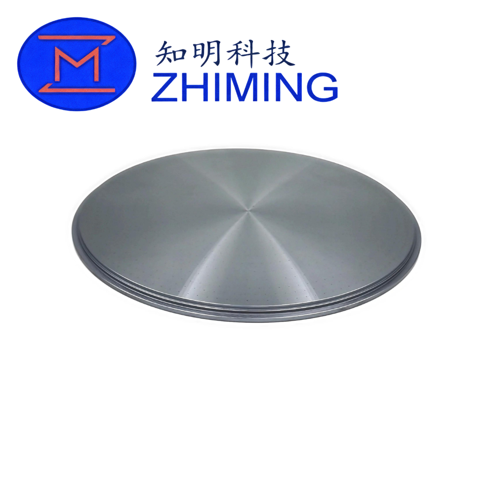
- 表面の柔軟性:用途に応じて、ポリッシュ仕上げ、ラップ仕上げ、研磨仕上げが可能。
技術仕様
| パラメータ | 仕様 |
|---|---|
| 素材 | 単結晶シリコン |
| 純度 | ≥ 99.999%(5N半導体グレード) |
| 直径(最大) | 480mmまで |
| 厚さ | カスタム(デザインにより通常5~50mm) |
| 抵抗率(低) | < 0.02 Ω-cm |
| 抵抗率(中) | 1 - 4 Ω-cm |
| 抵抗率(高) | 70 - 90 Ω-cm |
| 抵抗率の均一性 (RRG) | < 5% |
| ガスホール径 | 0.2~0.8mm(カスタマイズ可能) |
| 表面状態 | ポリッシュ/ラップ/研磨 |
| 表面粗さ(Ra) | ≤ 0.8 μm(研磨オプションは下側) |
| 加工精度 | < 10 μm |
| 平坦性 | ≤ 30 μm(サイズによる) |
| エッジ・プロフィール | カスタム面取り/半径 |
| 品質管理 | 欠け、ひび、傷、汚染なし |
アプリケーション
シリコン電極は、プラズマ相互作用が必要な半導体製造装置で広く使用されています。代表的な用途は以下の通りです:
- プラズマエッチング装置(ICP、RIE)
- 化学蒸着(CVD / PECVD)
- ウェハー表面処理プロセス
- 半導体チャンバー内部部品
- 静電またはプラズマ分配システム
プラズマの均一性を維持し、コンタミネーションを低減する能力により、成熟したプロセスノードでも先進的なプロセスノードでも不可欠なものとなっている。.
シリコン電極を選ぶ理由
シリコン電極は、コスト効率と性能のユニークなバランスを提供します。SiC部品に比べ、シリコン電極は経済的で機械加工が容易であるため、交換サイクルが許容されるアプリケーションに最適です。さらに、シリコンウェハープロセスとの本質的な互換性により、高いデバイス歩留まりを維持するために重要なクロスコンタミネーションのリスクを最小限に抑えることができます。.
より長い寿命や高い耐食性が要求される用途では、SiC電極が検討されるかもしれません。しかし、幅広い標準的な半導体プロセスでは、シリコン電極が業界標準のソリューションであり続けています。.
よくあるご質問
Q1: シリコン電極は消耗品ですか?
はい、重要な半導体消耗品に分類されます。プラズマへの暴露や化学反応により、徐々に摩耗し、定期的な交換が必要になります。.
Q2: どの抵抗率を選べばよいですか?
お客様のプロセス要件によります。低抵抗率は一般的に高い導電性が必要な場合に使用され、高抵抗率は絶縁や制御されたプラズマ環境に適しています。.
Q3: 電極はカスタマイズできますか?
はい。寸法、厚さ、ガスホールパターン、抵抗率、表面仕上げはすべて、お客様の図面や装置の要件に応じてカスタマイズできます。.

レビュー
レビューはまだありません。