
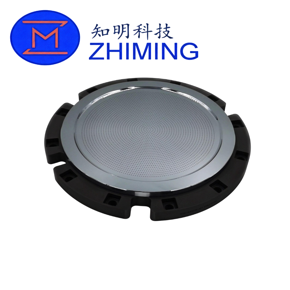
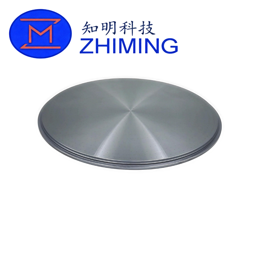
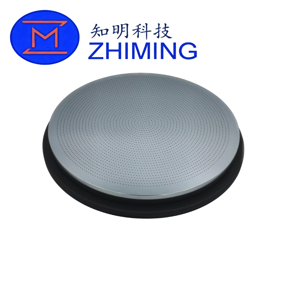
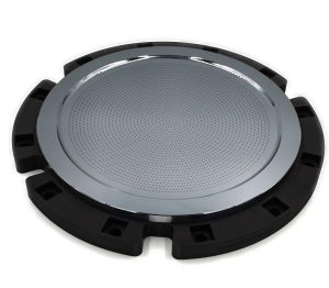
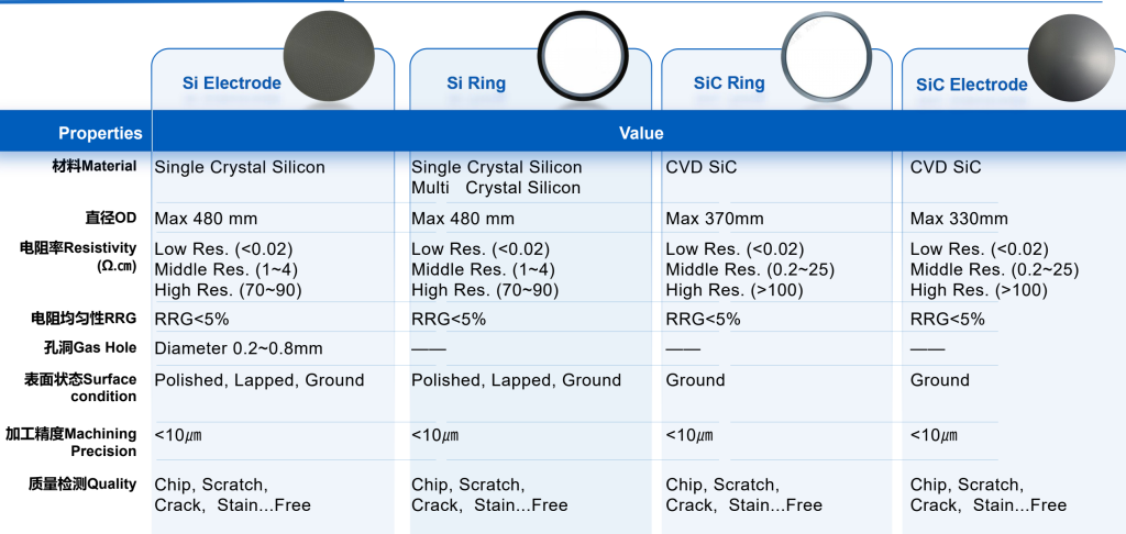
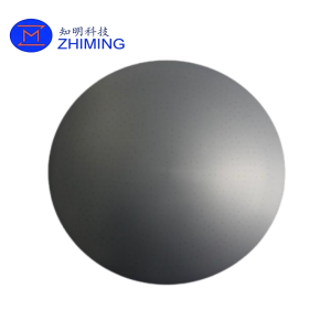
 Elektroda krzemowa jest podstawowym elementem funkcjonalnym stosowanym w zaawansowanych urządzeniach do przetwarzania plazmy półprzewodnikowej, w tym w systemach trawienia, osadzania i modyfikacji powierzchni. Wykonana z monokryształu krzemu o wysokiej czystości, odgrywa kluczową rolę w zapewnieniu stabilnego generowania plazmy, równomiernego rozkładu pola elektrycznego i precyzyjnego przetwarzania płytek.
W nowoczesnej produkcji półprzewodników stabilność procesu i wydajność są bezpośrednio zależne od wydajności wewnętrznych elementów komory. Elektrody krzemowe są powszechnie preferowane ze względu na ich doskonałą kompatybilność z procesami opartymi na krzemie, minimalizując ryzyko zanieczyszczenia i utrzymując wysoką czystość procesu. W porównaniu do elektrod metalowych, materiały krzemowe wykazują wyższą odporność na zanieczyszczenia wywołane plazmą i zapewniają bardziej spójne właściwości elektryczne.
Elektrody te są zwykle używane w trudnych warunkach, w których występuje plazma o wysokiej energii, gazy reaktywne, takie jak CF₄, SF₆ i Cl₂, oraz podwyższone temperatury. Z czasem ulegają one stopniowej erozji i dlatego są klasyfikowane jako krytyczne półprzewodnikowe materiały eksploatacyjne, wymagające okresowej wymiany przy zachowaniu wysokiej wydajności przez cały okres eksploatacji.
Kluczowe cechy
- Materiał o wysokiej czystości: Wykonane z półprzewodnikowego krzemu monokrystalicznego, aby zapewnić minimalną ilość zanieczyszczeń i stabilne parametry elektryczne.
- Wiele opcji rezystywności: Dostępne w klasach o niskiej, średniej i wysokiej rezystywności dla różnych wymagań kontroli plazmy.
- Doskonała kompatybilność z plazmą: Zmniejsza wytwarzanie cząstek i poprawia wydajność wafli
- Obróbka precyzyjna: Wąskie tolerancje (<10 μm) dla integracji wysokiej klasy sprzętu półprzewodnikowego
- Niestandardowa konstrukcja otworu gazowego: Zapewnia równomierną dystrybucję gazu i zoptymalizowaną gęstość plazmy
- Elastyczność powierzchni: Dostępne w wykończeniu polerowanym, docieranym lub szlifowanym w zależności od potrzeb.
Specyfikacja techniczna
| Parametr | Specyfikacja |
|---|---|
| Materiał | Pojedynczy kryształ krzemu |
| Czystość | ≥ 99,999% (klasa półprzewodnikowa 5N) |
| Średnica (maks.) | Do 480 mm |
| Grubość | Niestandardowe (zazwyczaj 5-50 mm w zależności od projektu) |
| Rezystywność (niska) | < 0,02 Ω-cm |
| Rezystywność (średnia) | 1 - 4 Ω-cm |
| Rezystywność (wysoka) | 70 - 90 Ω-cm |
| Jednorodność rezystywności (RRG) | < 5% |
| Średnica otworu gazowego | 0,2 - 0,8 mm (z możliwością dostosowania) |
| Stan powierzchni | Polerowane / docierane / szlifowane |
| Chropowatość powierzchni (Ra) | ≤ 0,8 μm (niższa opcja polerowana) |
| Precyzja obróbki | < 10 μm |
| Płaskość | ≤ 30 μm (w zależności od rozmiaru) |
| Profil krawędzi | Niestandardowa faza / promień |
| Kontrola jakości | Bez odprysków, pęknięć, zarysowań, zanieczyszczeń |
Zastosowania
Elektrody krzemowe są szeroko stosowane w urządzeniach do produkcji półprzewodników, gdzie wymagana jest interakcja plazmy. Typowe zastosowania obejmują:
- Systemy trawienia plazmowego (ICP, RIE)
- Chemiczne osadzanie z fazy gazowej (CVD / PECVD)
- Procesy obróbki powierzchni wafli
- Elementy wewnętrzne komory półprzewodnikowej
- Systemy dystrybucji elektrostatycznej lub plazmowej
Ich zdolność do utrzymania jednorodności plazmy i zmniejszenia zanieczyszczenia sprawia, że są one niezbędne zarówno w dojrzałych, jak i zaawansowanych węzłach procesowych.
Dlaczego warto wybrać elektrody krzemowe?
Elektrody krzemowe oferują wyjątkową równowagę między efektywnością kosztową a wydajnością. W porównaniu do komponentów SiC, elektrody krzemowe są bardziej ekonomiczne i łatwiejsze w obróbce, co czyni je idealnymi do zastosowań, w których dopuszczalne są cykle wymiany. Dodatkowo, ich wewnętrzna kompatybilność z procesami wafli krzemowych zapewnia minimalne ryzyko zanieczyszczenia krzyżowego, co ma kluczowe znaczenie dla utrzymania wysokiej wydajności urządzeń.
W przypadku zastosowań wymagających dłuższej żywotności lub wyższej odporności na korozję można rozważyć elektrody SiC. Jednak w przypadku szerokiej gamy standardowych procesów półprzewodnikowych, elektrody krzemowe pozostają standardowym rozwiązaniem w branży.
FAQ
P1: Czy elektroda krzemowa jest częścią eksploatacyjną?
Tak, jest klasyfikowany jako krytyczny półprzewodnikowy materiał eksploatacyjny. Ze względu na ekspozycję na działanie plazmy i reakcje chemiczne stopniowo się zużywa i wymaga okresowej wymiany.
P2: Jaką rezystywność powinienem wybrać?
Zależy to od wymagań procesowych. Niska rezystywność jest zwykle stosowana w przypadku wyższych wymagań dotyczących przewodności, podczas gdy wysoka rezystywność jest odpowiednia do izolacji i kontrolowanych środowisk plazmowych.
P3: Czy elektrodę można dostosować?
Tak. Wymiary, grubość, wzory otworów gazowych, rezystywność i wykończenie powierzchni można dostosować zgodnie z rysunkami lub wymaganiami sprzętowymi.


Opinie
Na razie nie ma opinii o produkcie.