
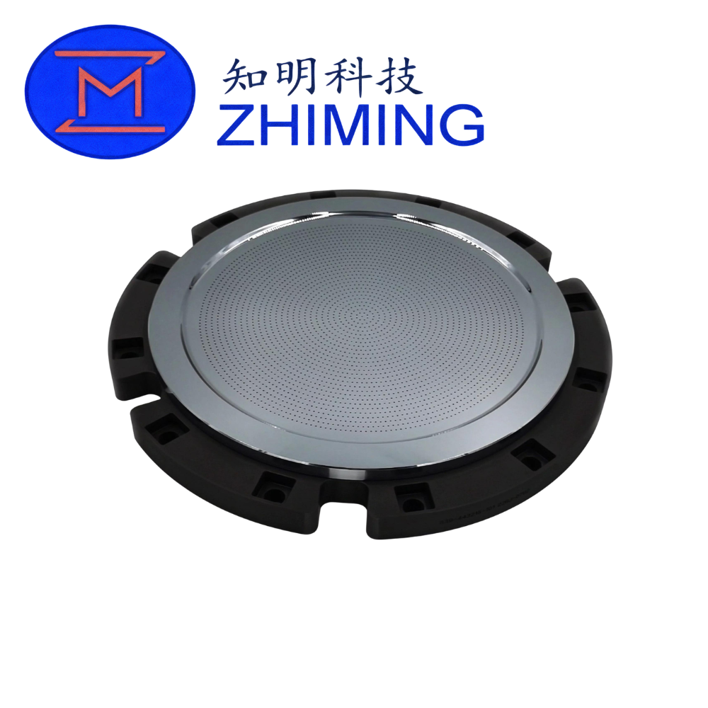
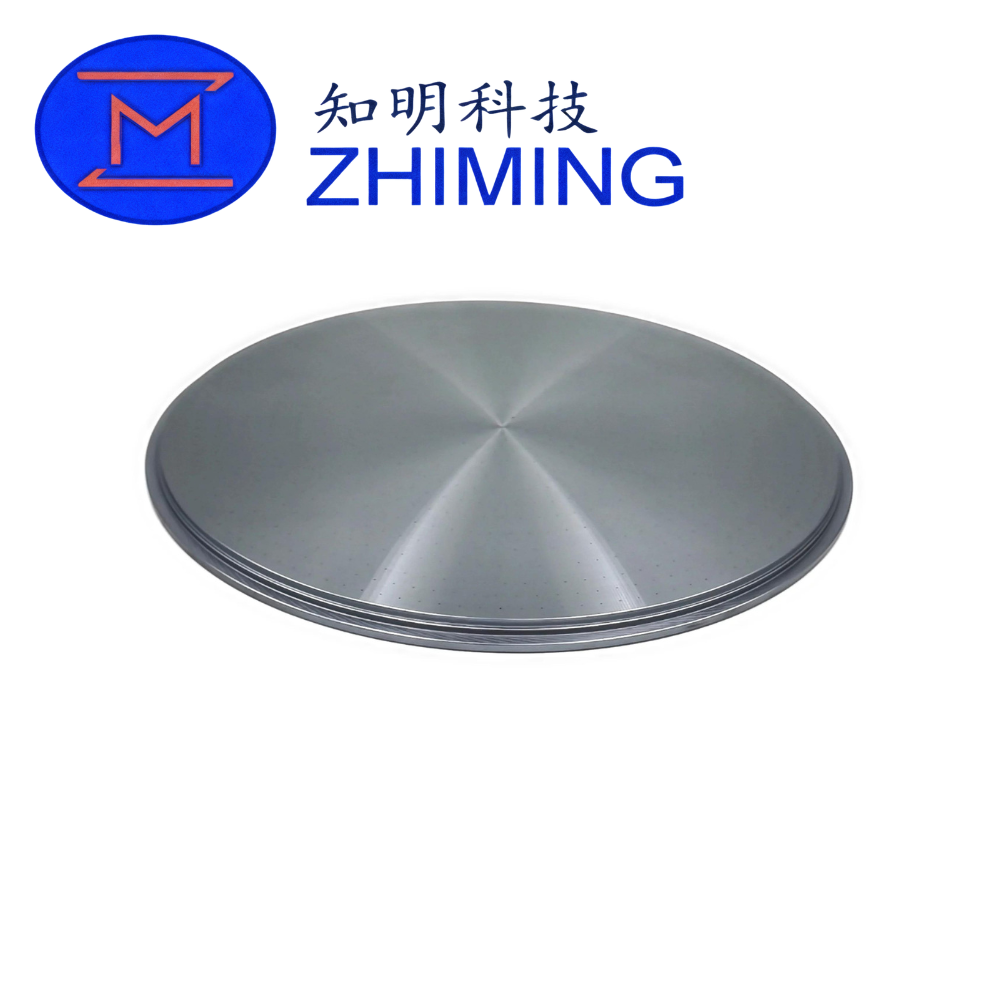
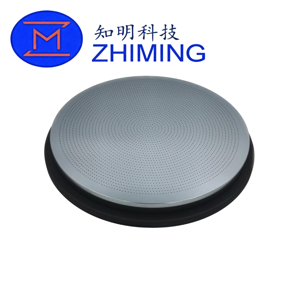
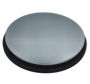
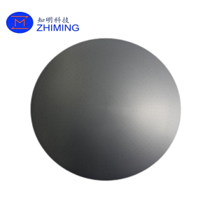
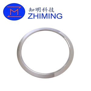
 실리콘 전극은 에칭, 증착, 표면 개질 시스템 등 첨단 반도체 플라즈마 처리 장비에 사용되는 핵심 기능 부품입니다. 고순도 단결정 실리콘으로 제조되어 안정적인 플라즈마 생성, 균일한 전기장 분포, 정밀한 웨이퍼 가공을 보장하는 데 중요한 역할을 합니다.
최신 반도체 제조에서 공정 안정성과 수율은 내부 챔버 구성 요소의 성능에 직접적인 영향을 받습니다. 실리콘 전극은 실리콘 기반 공정과의 호환성이 뛰어나 오염 위험을 최소화하고 높은 공정 순도를 유지하기 때문에 널리 선호됩니다. 금속 전극에 비해 실리콘 소재는 플라즈마로 인한 오염에 대한 저항성이 우수하고 전기적 특성이 더욱 일관되게 유지됩니다.
이러한 전극은 일반적으로 고에너지 플라즈마, CF₄, SF₆, Cl₂와 같은 반응성 가스, 높은 온도와 관련된 열악한 환경에서 사용됩니다. 시간이 지남에 따라 점진적으로 침식되므로 다음과 같이 분류됩니다. 중요 반도체 소모품, 수명 주기 내내 고성능을 유지하면서 주기적으로 교체해야 합니다.
주요 기능
- 고순도 소재: 반도체 등급의 단결정 실리콘으로 제작되어 불순물을 최소화하고 안정적인 전기적 성능을 보장합니다.
- 다양한 저항률 옵션: 다양한 플라즈마 제어 요구 사항에 따라 저, 중, 고 저항 등급으로 제공됩니다.
- 뛰어난 플라즈마 호환성: 입자 생성 감소 및 웨이퍼 수율 향상
- 정밀 가공: 하이엔드 반도체 장비 통합을 위한 엄격한 허용 오차(<10μm)
- 맞춤형 가스 홀 디자인: 균일한 가스 분포 및 최적화된 플라즈마 밀도 지원
- 표면 유연성: 용도에 따라 광택, 랩 또는 연마 마감으로 제공 가능
기술 사양
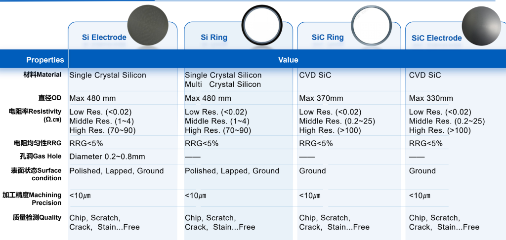
| 매개변수 | 사양 |
|---|---|
| 재료 | 단결정 실리콘 |
| 순도 | ≥ 99.999%(5N 반도체 등급) |
| 지름(최대) | 최대 480mm |
| 두께 | 사용자 지정(디자인에 따라 일반적으로 5~50mm) |
| 저항률(낮음) | < 0.02 Ω-cm |
| 저항률(중간) | 1 - 4 Ω-cm |
| 저항률(높음) | 70 - 90 Ω-cm |
| 저항률 균일성(RRG) | < 5% |
| 가스 구멍 지름 | 0.2 - 0.8mm(사용자 지정 가능) |
| 표면 상태 | 광택 / 랩핑 / 그라운드 |
| 표면 거칠기(Ra) | ≤ 0.8μm(광택 옵션 하단) |
| 가공 정밀도 | < 10μm 미만 |
| 평탄도 | ≤ 30μm(크기에 따라 다름) |
| 엣지 프로필 | 맞춤형 모따기 / 반경 |
| 품질 관리 | 칩, 균열, 긁힘, 오염 없음 |
애플리케이션
실리콘 전극은 플라즈마 상호 작용이 필요한 반도체 제조 장비에 널리 사용됩니다. 일반적인 응용 분야는 다음과 같습니다:
- 플라즈마 에칭 시스템(ICP, RIE)
- 화학 기상 증착(CVD/PECVD)
- 웨이퍼 표면 처리 공정
- 반도체 챔버 내부 구성 요소
- 정전기 또는 플라즈마 분배 시스템
플라즈마 균일성을 유지하고 오염을 줄이는 능력은 성숙 및 고급 공정 노드 모두에서 필수적입니다.
왜 실리콘 전극을 선택해야 할까요?
실리콘 전극은 비용 효율성과 성능 사이의 독특한 균형을 제공합니다. 실리콘 전극은 SiC 부품에 비해 경제적이고 가공하기 쉬우므로 교체 주기가 허용되는 애플리케이션에 이상적입니다. 또한 실리콘 웨이퍼 공정과의 본질적인 호환성으로 인해 교차 오염의 위험을 최소화할 수 있어 높은 디바이스 수율을 유지하는 데 매우 중요합니다.
더 긴 수명 또는 더 높은 내식성이 필요한 애플리케이션의 경우 SiC 전극을 고려할 수 있습니다. 그러나 광범위한 표준 반도체 공정의 경우 실리콘 전극이 여전히 업계 표준 솔루션으로 사용되고 있습니다.
자주 묻는 질문
Q1: 실리콘 전극은 소모품인가요?
예, 반도체 핵심 소모품으로 분류됩니다. 플라즈마 노출과 화학 반응으로 인해 서서히 마모되어 주기적으로 교체해야 합니다.
Q2: 어떤 저항을 선택해야 하나요?
공정 요구 사항에 따라 다릅니다. 낮은 저항률은 일반적으로 높은 전도성이 필요한 경우에 사용되며, 높은 저항률은 절연 및 제어 플라즈마 환경에 적합합니다.
Q3: 전극을 사용자 지정할 수 있나요?
예. 도면 또는 장비 요구 사항에 따라 치수, 두께, 가스 구멍 패턴, 저항률 및 표면 마감을 모두 맞춤 설정할 수 있습니다.

상품평
아직 상품평이 없습니다.