
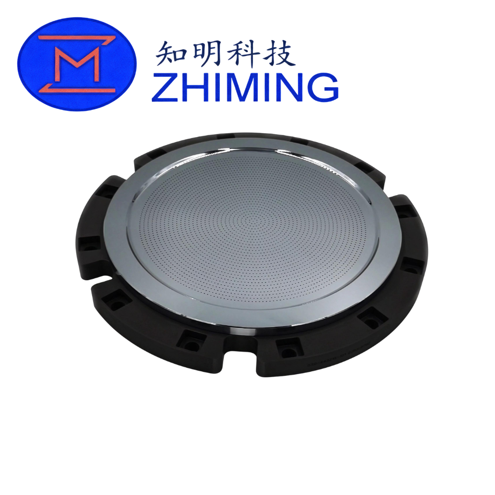
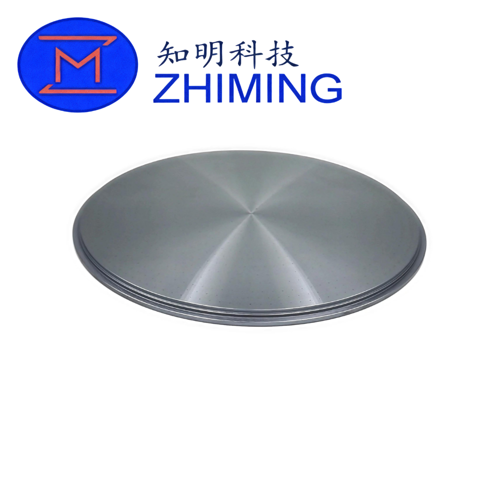
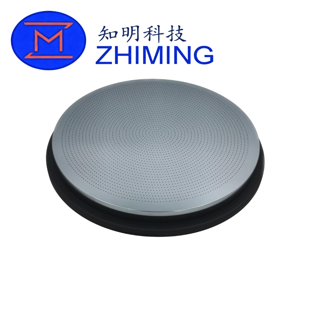
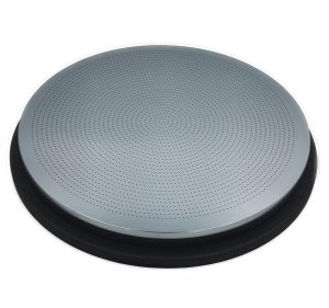
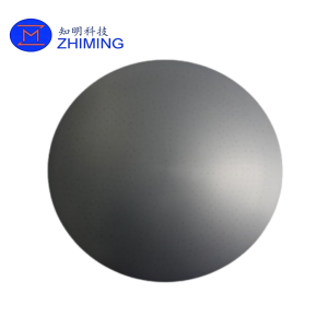
 Kiselelektroden är en central funktionell komponent som används i avancerad utrustning för plasmabehandling av halvledare, inklusive system för etsning, deponering och ytmodifiering. Den tillverkas av enkristallint kisel med hög renhet och spelar en avgörande roll för att säkerställa stabil plasmagenerering, enhetlig elektrisk fältfördelning och exakt waferbearbetning.
I modern halvledartillverkning påverkas processtabilitet och utbyte direkt av prestandan hos de interna kammarkomponenterna. Kiselelektroder är allmänt föredragna på grund av deras utmärkta kompatibilitet med kiselbaserade processer, vilket minimerar kontamineringsrisker och upprätthåller hög processrenhet. Jämfört med metallelektroder uppvisar kiselmaterial överlägsen motståndskraft mot plasmainducerad kontaminering och ger mer konsekventa elektriska egenskaper.
Dessa elektroder används vanligtvis i tuffa miljöer med plasma med hög energi, reaktiva gaser som CF₄, SF₆ och Cl₂ samt förhöjda temperaturer. Med tiden genomgår de en gradvis erosion och klassificeras därför som kritiska förbrukningsvaror för halvledare, De behöver inte bytas ut med jämna mellanrum samtidigt som de bibehåller hög prestanda under hela sin livscykel.
Viktiga funktioner
- Material med hög renhet: Tillverkad av enkristallint kisel av halvledarkvalitet för att säkerställa minimala föroreningar och stabil elektrisk prestanda
- Flera alternativ för resistivitet: Finns i kvaliteter med låg, medelhög och hög resistivitet för olika krav på plasmakontroll
- Utmärkt plasmakompatibilitet: Minskar partikelgenerering och förbättrar waferutbytet
- Precisionsbearbetning: Snäva toleranser (<10 μm) för integration av avancerade halvledarutrustningar
- Anpassad design av gashål: Stödjer enhetlig gasfördelning och optimerad plasmatäthet
- Ytans flexibilitet: Finns i polerad, lappad eller slipad finish beroende på applikationens behov
Tekniska specifikationer
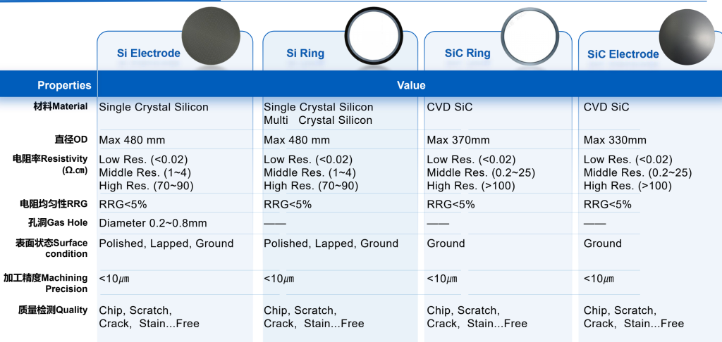
| Parameter | Specifikation |
|---|---|
| Material | Enkristallkisel |
| Renhet | ≥ 99,999% (5N halvledarkvalitet) |
| Diameter (max) | Upp till 480 mm |
| Tjocklek | Anpassad (typiskt 5-50 mm beroende på design) |
| Resistivitet (låg) | < 0,02 Ω-cm |
| Resistivitet (Medium) | 1 - 4 Ω-cm |
| Resistivitet (hög) | 70 - 90 Ω-cm |
| Enhetlig resistivitet (RRG) | < 5% |
| Håldiameter för gas | 0,2 - 0,8 mm (anpassningsbar) |
| Ytans tillstånd | Polerad / Lappad / Slipad |
| Ytjämnhet (Ra) | ≤ 0,8 μm (polerat alternativ lägre) |
| Maskinbearbetning Precision | < 10 μm |
| Planhet | ≤ 30 μm (beroende på storlek) |
| Kantprofil | Anpassad avfasning/radie |
| Kvalitetskontroll | Fri från chip, sprickor, repor och föroreningar |
Tillämpningar
Kiselelektroder används ofta i utrustning för halvledartillverkning där plasmainteraktion krävs. Typiska applikationer inkluderar:
- System för plasmaetsning (ICP, RIE)
- Kemisk förångningsdeposition (CVD/PECVD)
- Processer för ytbehandling av wafers
- Halvledarkammarens interna komponenter
- Elektrostatiska eller plasmafördelningssystem
Deras förmåga att hålla plasmat enhetligt och minska kontamineringen gör dem viktiga i både mogna och avancerade processnoder.
Varför välja kiselelektroder?
Kiselelektroder erbjuder en unik balans mellan kostnadseffektivitet och prestanda. Jämfört med SiC-komponenter är kiselelektroder mer ekonomiska och enklare att bearbeta, vilket gör dem idealiska för applikationer där utbytescyklerna är acceptabla. Dessutom säkerställer deras inneboende kompatibilitet med kiselskiveprocesser minimal risk för korskontaminering, vilket är avgörande för att upprätthålla höga enhetsutbyten.
För applikationer som kräver längre livslängd eller högre korrosionsbeständighet kan SiC-elektroder övervägas. För ett stort antal standardprocesser inom halvledarområdet är dock kiselelektroder fortfarande industristandard.
VANLIGA FRÅGOR
F1: Är kiselelektroden en förbrukningsvara?
Ja, den är klassificerad som en kritisk halvledarförbrukningsprodukt. På grund av plasmaexponering och kemiska reaktioner slits den gradvis och måste bytas ut med jämna mellanrum.
F2: Vilken resistivitet ska jag välja?
Det beror på dina processkrav. Låg resistivitet används vanligtvis för behov av högre ledningsförmåga, medan hög resistivitet är lämplig för isolering och kontrollerade plasmamiljöer.
F3: Kan elektroden anpassas?
Ja, det kan vi. Mått, tjocklek, gashålsmönster, resistivitet och ytfinish kan alla anpassas efter dina ritningar eller utrustningskrav.

Recensioner
Det finns inga recensioner än.