
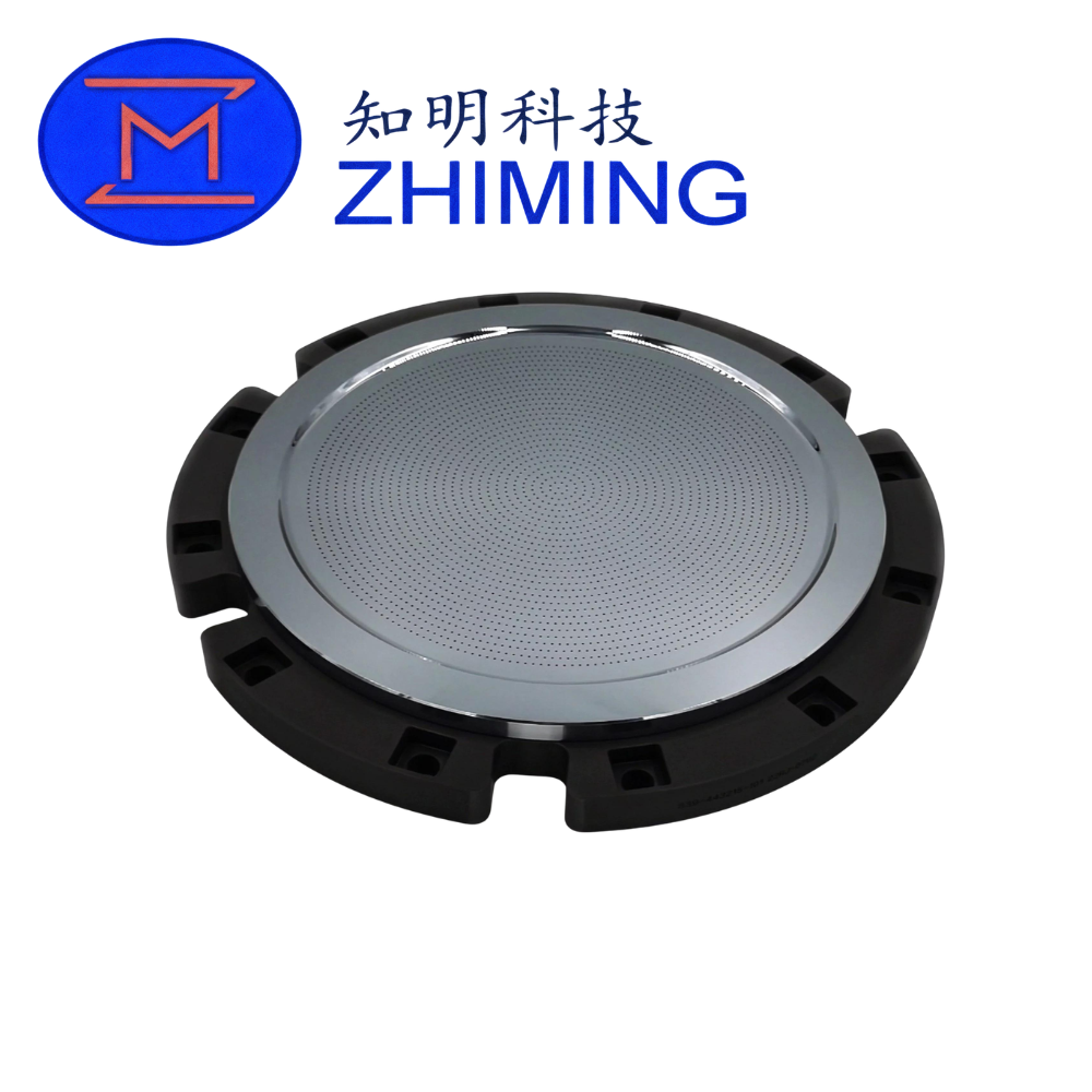
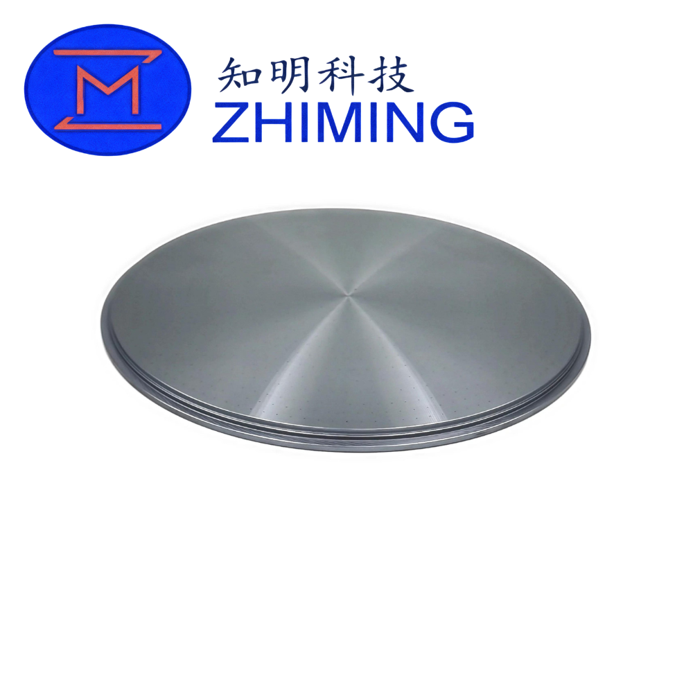
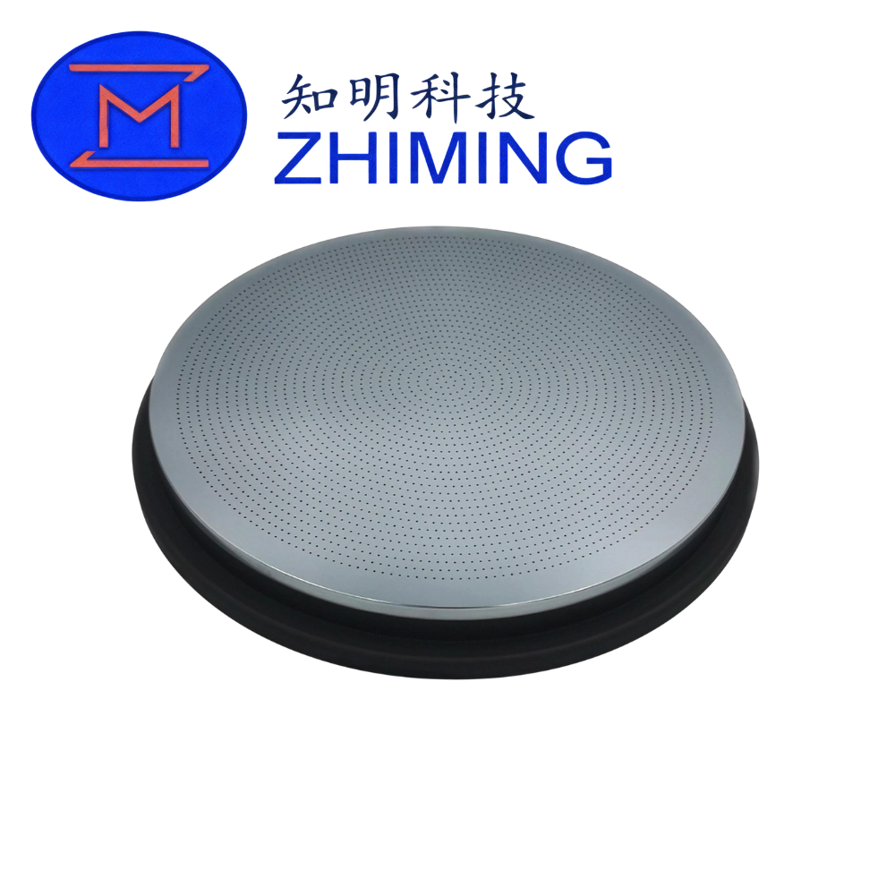
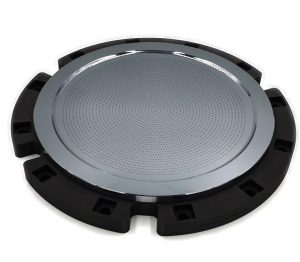
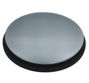
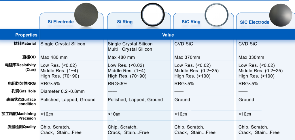
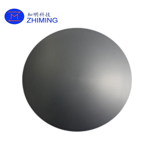
 The silicon electrode is a core functional component used in advanced semiconductor plasma processing equipment, including etching, deposition, and surface modification systems. Manufactured from high-purity single crystal silicon, it plays a critical role in ensuring stable plasma generation, uniform electric field distribution, and precise wafer processing.
In modern semiconductor fabrication, process stability and yield are directly affected by the performance of internal chamber components. Silicon electrodes are widely preferred due to their excellent compatibility with silicon-based processes, minimizing contamination risks and maintaining high process purity. Compared to metal electrodes, silicon materials exhibit superior resistance to plasma-induced contamination and provide more consistent electrical characteristics.
These electrodes are typically used in harsh environments involving high-energy plasma, reactive gases such as CF₄, SF₆, and Cl₂, and elevated temperatures. Over time, they undergo gradual erosion and are therefore classified as critical semiconductor consumables, requiring periodic replacement while maintaining high performance throughout their lifecycle.
Key Features
- High Purity Material: Made from semiconductor-grade single crystal silicon to ensure minimal impurities and stable electrical performance
- Multiple Resistivity Options: Available in low, medium, and high resistivity grades for different plasma control requirements
- Excellent Plasma Compatibility: Reduces particle generation and improves wafer yield
- Precision Machining: Tight tolerances (<10 μm) for high-end semiconductor equipment integration
- Custom Gas Hole Design: Supports uniform gas distribution and optimized plasma density
- Surface Flexibility: Available in polished, lapped, or ground finishes based on application needs
Technical Specifications
| Parameter | Specification |
|---|---|
| Material | Single Crystal Silicon |
| Purity | ≥ 99.999% (5N semiconductor grade) |
| Diameter (Max) | Up to 480 mm |
| Thickness | Custom (typically 5–50 mm depending on design) |
| Resistivity (Low) | < 0.02 Ω·cm |
| Resistivity (Medium) | 1 – 4 Ω·cm |
| Resistivity (High) | 70 – 90 Ω·cm |
| Resistivity Uniformity (RRG) | < 5% |
| Gas Hole Diameter | 0.2 – 0.8 mm (customizable) |
| Surface Condition | Polished / Lapped / Ground |
| Surface Roughness (Ra) | ≤ 0.8 μm (polished option lower) |
| Machining Precision | < 10 μm |
| Flatness | ≤ 30 μm (depending on size) |
| Edge Profile | Custom chamfer / radius |
| Quality Control | Free of chip, crack, scratch, contamination |
Applications
Silicon electrodes are widely used in semiconductor manufacturing equipment where plasma interaction is required. Typical applications include:
- Plasma etching systems (ICP, RIE)
- Chemical vapor deposition (CVD / PECVD)
- Wafer surface treatment processes
- Semiconductor chamber internal components
- Electrostatic or plasma distribution systems
Their ability to maintain plasma uniformity and reduce contamination makes them essential in both mature and advanced process nodes.
Why Choose Silicon Electrodes?
Silicon electrodes offer a unique balance between cost efficiency and performance. Compared to SiC components, silicon electrodes are more economical and easier to machine, making them ideal for applications where replacement cycles are acceptable. Additionally, their intrinsic compatibility with silicon wafer processes ensures minimal risk of cross-contamination, which is critical for maintaining high device yields.
For applications requiring longer lifetime or higher corrosion resistance, SiC electrodes may be considered. However, for a wide range of standard semiconductor processes, silicon electrodes remain the industry-standard solution.
FAQ
Q1: Is the silicon electrode a consumable part?
Yes, it is classified as a critical semiconductor consumable. Due to plasma exposure and chemical reactions, it gradually wears and requires periodic replacement.
Q2: What resistivity should I choose?
It depends on your process requirements. Low resistivity is typically used for higher conductivity needs, while high resistivity is suitable for insulation and controlled plasma environments.
Q3: Can the electrode be customized?
Yes. Dimensions, thickness, gas hole patterns, resistivity, and surface finish can all be customized according to your drawings or equipment requirements.

Reviews
There are no reviews yet.