
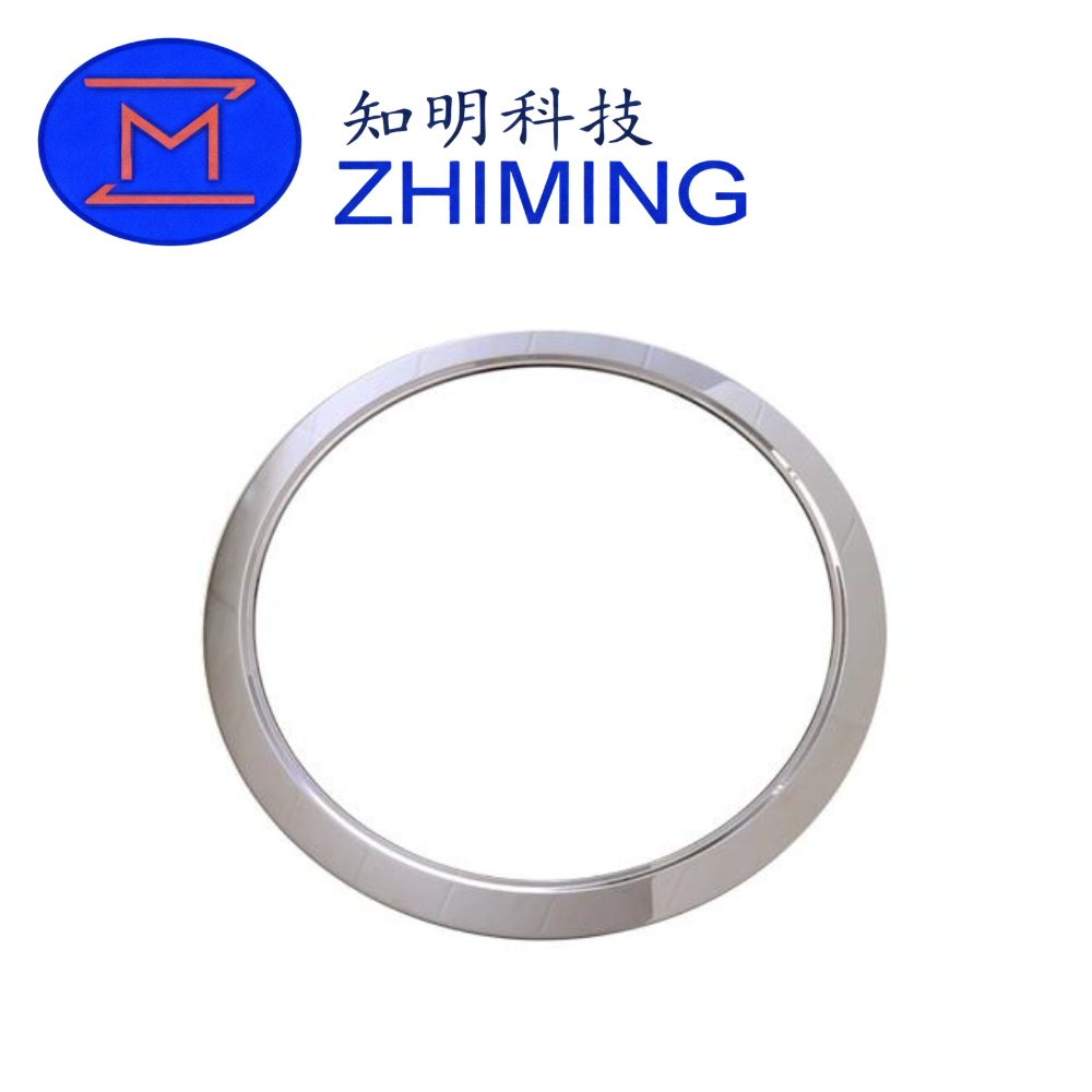
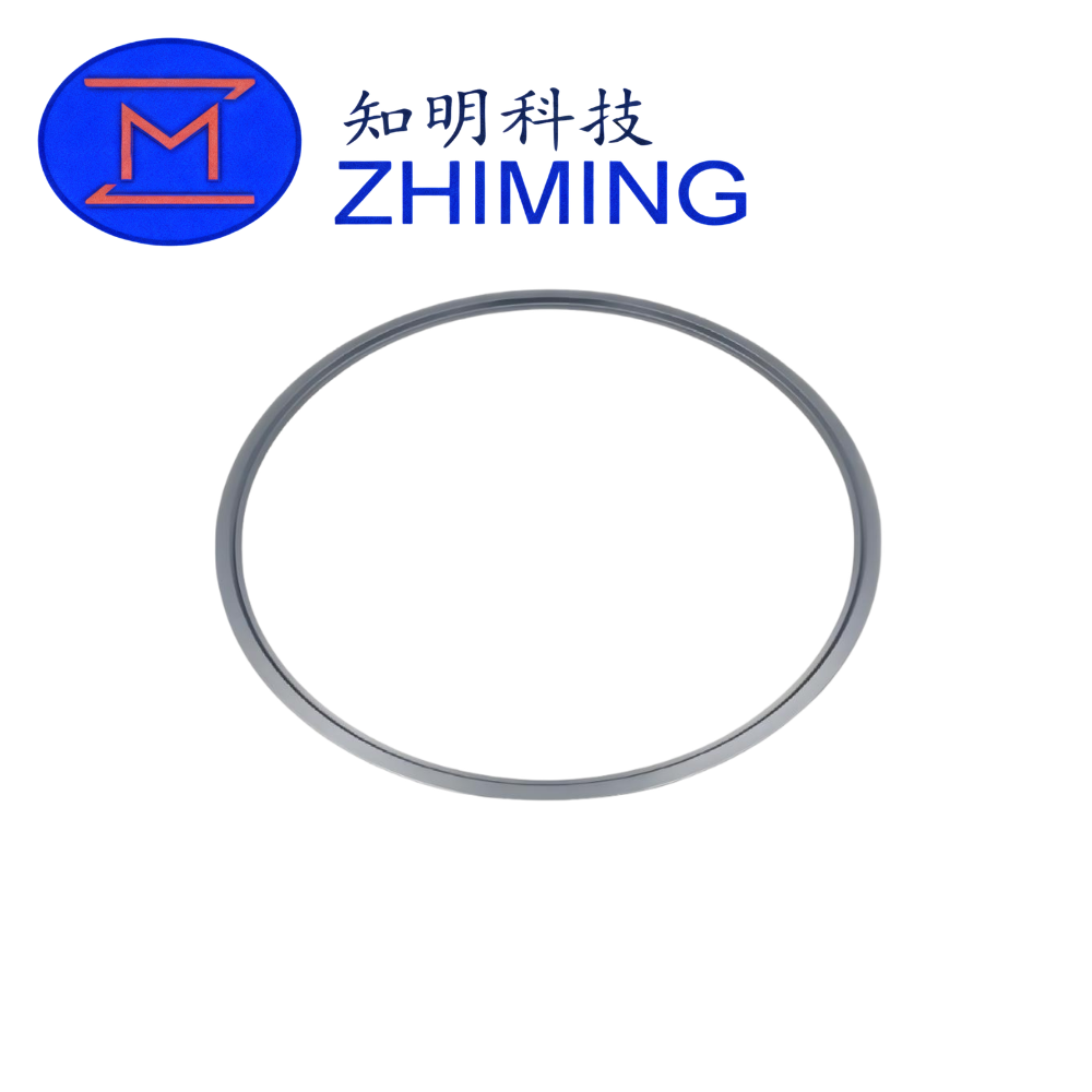
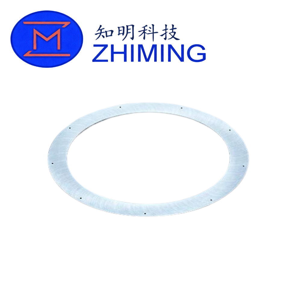
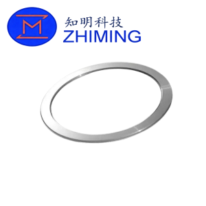
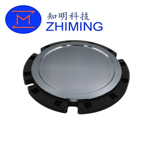
 The Silicon Ring (Si Ring) is a widely used component in semiconductor plasma processing equipment, serving as a focus ring, edge ring, or chamber liner. It plays a key role in controlling plasma distribution, improving etching uniformity, and protecting critical chamber components from direct exposure to high-energy plasma.
Manufactured from high-purity single crystal silicon or polycrystalline silicon, Si rings offer excellent compatibility with silicon wafer processes. This intrinsic material compatibility significantly reduces contamination risks, making silicon rings a preferred choice in many semiconductor fabrication environments.
During operation, silicon rings are exposed to reactive plasma generated by gases such as CF₄, SF₆, NF₃, and Cl₂. These conditions gradually cause material erosion and surface degradation. As a result, silicon rings are classified as critical semiconductor consumables, requiring periodic replacement to maintain optimal process performance and yield.
Compared to SiC rings, silicon rings are more cost-effective and easier to machine, making them ideal for applications where replacement cycles are acceptable and cost control is important.
Key Features
- High Purity Silicon Material: Available in single crystal and polycrystalline forms
- Excellent Process Compatibility: Ideal for silicon wafer processing with low contamination risk
- Stable Electrical Properties: Supports consistent plasma behavior
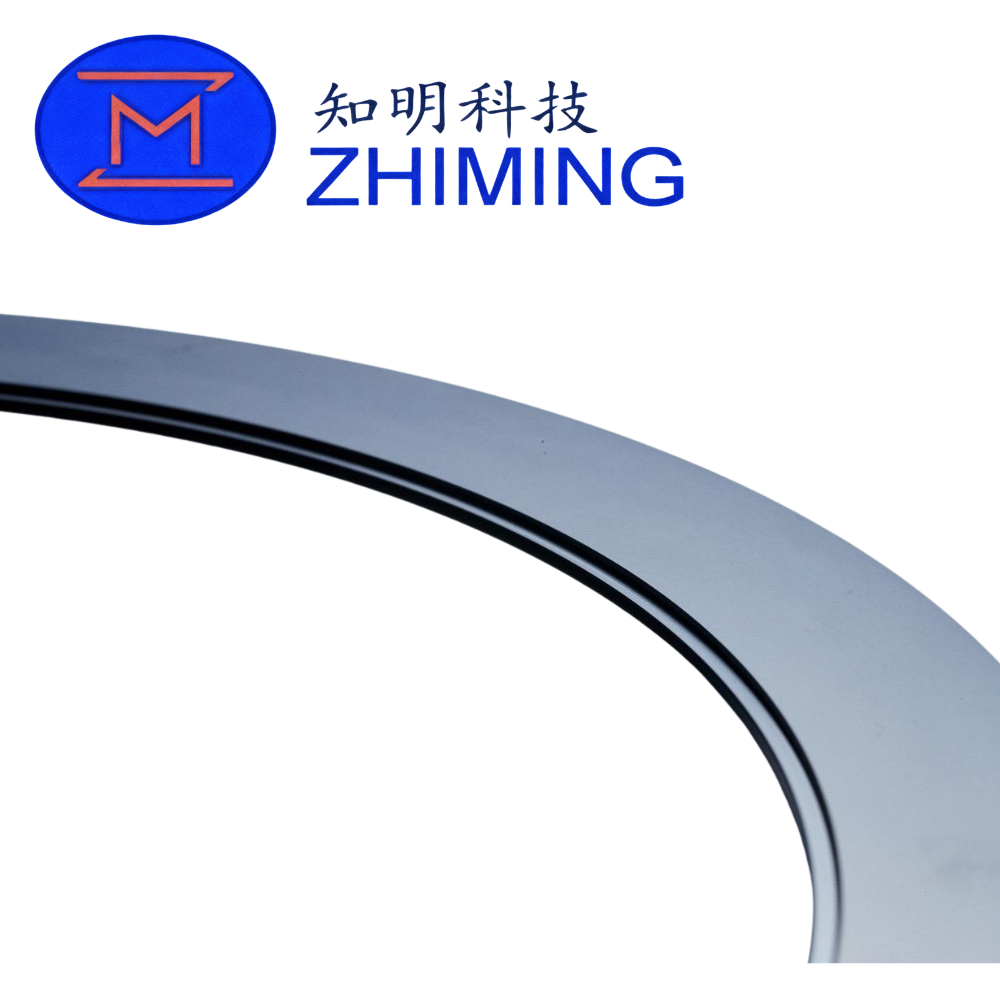
- Precision Machining: Tight tolerance (<10 μm) for advanced semiconductor tools
- Multiple Resistivity Options: Suitable for different plasma control requirements
- Cost-Effective Solution: Lower initial cost compared to SiC alternatives
- Custom Design Support: Complex geometries and sizes available
Technical Specifications
| Parameter | Specification |
|---|---|
| Material | Single Crystal Silicon / Polycrystalline Silicon |
| Purity | ≥ 99.999% (5N semiconductor grade) |
| Diameter (Max) | Up to 480 mm |
| Thickness | Custom (typically 5–30 mm) |
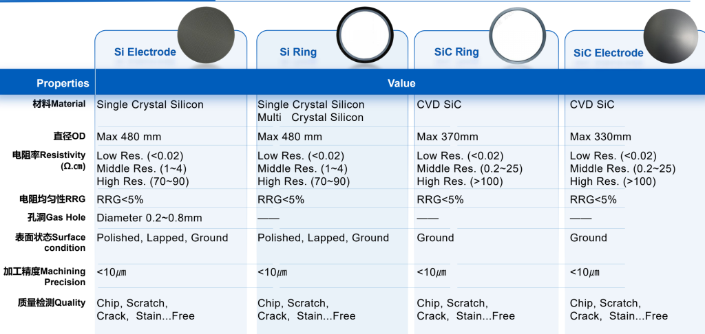
| Resistivity (Low) | < 0.02 Ω·cm |
| Resistivity (Medium) | 1 – 4 Ω·cm |
| Resistivity (High) | 70 – 90 Ω·cm |
| Resistivity Uniformity (RRG) | < 5% |
| Surface Condition | Polished / Lapped / Ground |
| Surface Roughness (Ra) | ≤ 0.8 μm (polished can be lower) |
| Machining Precision | < 10 μm |
| Flatness | ≤ 30 μm (depending on size) |
| Edge Type | Chamfer / Radius customizable |
| Quality Control | No cracks, chips, scratches, contamination |
Applications
Silicon rings are essential in a variety of semiconductor processing environments:
- Plasma etching systems (ICP / RIE)
- Chemical vapor deposition (CVD / PECVD)
- Focus ring / edge ring components
- Chamber protection and lining parts
- Wafer edge plasma control applications
They are widely used in both mature and intermediate process nodes where cost efficiency and stable performance are required.
Advantages & Positioning
Silicon rings provide a balanced solution between performance and cost. Compared with SiC rings:
- Lower Cost: Ideal for budget-sensitive or high-replacement scenarios
- Good Process Compatibility: Especially suitable for silicon-based processes
- Flexible Manufacturing: Easier to machine into complex designs
- Reliable Performance: Proven in large-scale semiconductor production
However, under extremely harsh plasma conditions, silicon rings may wear faster than SiC rings. Therefore, material selection should be based on process intensity, lifetime expectations, and cost considerations.
FAQ
Q1: Is the silicon ring a consumable product?
Yes. It is considered a critical semiconductor consumable due to gradual erosion in plasma environments.
Q2: What is the difference between single crystal and polycrystalline silicon rings?
Single crystal silicon offers better uniformity and electrical properties, while polycrystalline silicon is more cost-effective.
Q3: Can the silicon ring be customized?
Yes. Size, thickness, resistivity, surface finish, and geometry can all be customized according to your drawings.
Q4: How often does a silicon ring need replacement?
It depends on process conditions, but typically more frequently than SiC rings due to lower plasma resistance.
Q5: What is the typical lead time?
Production generally takes 3–5 weeks depending on specifications and quantity.
Reviews
There are no reviews yet.