
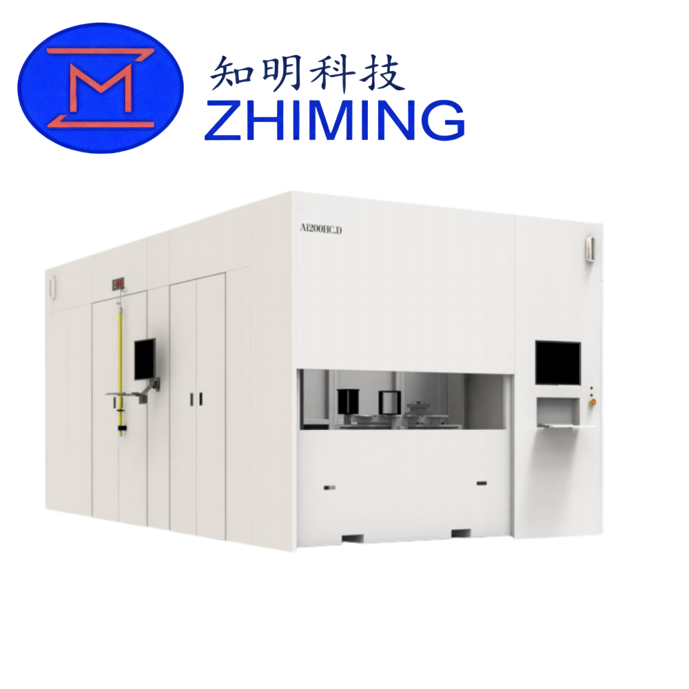
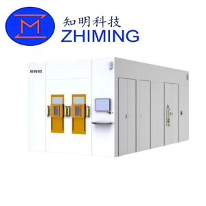
 Ai200HC.D (High Beam) iyon implantasyon sistemi, 6 inç ve 8 inç silikon gofret yarı iletken üretim hatları için tasarlanmıştır. Entegre devre üretiminde hassas doping ve ileri proses uygulamaları için geliştirilmiş yüksek akımlı bir iyon implanteridir.
Sistem, 5 keV ila 180 keV enerji aralığını destekleyerek istikrarlı ışın performansı ve yüksek proses tekrarlanabilirliği sağlar. Smart Cut teknolojisi entegrasyonu da dahil olmak üzere silikon bazlı yarı iletken üretimi ve gelişmiş wafer bonding ile ilgili süreçler için uygundur.
Özellikler
Yüksek Işın Stabilite Performansı
Sistem, kontrollü dalgalanma ile istikrarlı iyon ışını çıkışını koruyarak sürekli üretim sırasında tutarlı implantasyon kalitesi sağlar.
Geniş Süreç Uyumluluğu
Silikon bazlı prosesler ve Smart Cut ile ilgili uygulamalarla uyumludur ve gelişmiş wafer mühendisliği gereksinimlerini destekler.
Yüksek Hassasiyetli İmplant Kontrolü
ile doğru implantasyon performansı sağlar:
- Açı doğruluğu ≤ 0,2°
- Kiriş paralelliği ≤ 0,3°
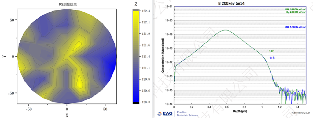
- Tekdüzelik ≤ 1%
- Tekrarlanabilirlik ≤ 1%
Yüksek Verim Kapasitesi
Saatte ≥ 220 wafer destekler, orta ve yüksek hacimli yarı iletken üretim ortamları için uygundur.
Toplu Hedef İşleme Yeteneği
Toplu hedef işlemeyi destekler, süreç esnekliğini artırır ve gelişmiş silikon yonga plakası üretim teknolojileriyle entegrasyon sağlar.
Temel Özellikler
Süreç Parametreleri
| Öğe | Şartname |
|---|---|
| Gofret Boyutu | 6-8 inç silikon gofretler |
| Enerji Aralığı | 5-180 keV |
| İmplante Edilmiş Elemanlar | B+, BF2+, P+, As+, N+, H+ |
| Doz Aralığı | 5E11-1E17 iyon/cm² |
Işın Performansı
| Öğe | Şartname |
|---|---|
| Kiriş Stabilitesi | ≤ Saat başına 10% |
| Kiriş Paralelliği | ≤ 0.3° |
İmplantasyon Doğruluğu
| Öğe | Şartname |
|---|---|
| İmplant Açı Aralığı | -11° ila 11° |
| Açı Doğruluğu | ≤ 0.2° |
| Tekdüzelik (1σ) | ≤ 1% (B+, 2E14, 150 keV) |
| Tekrarlanabilirlik (1σ) | ≤ 1% (B+, 2E14, 150 keV) |
Sistem Performansı
| Öğe | Şartname |
|---|---|
| Verim | Saatte ≥ 220 gofret |
| Ekipman Boyutu | 5930 × 3000 × 2630 mm |
Uygulama
Silikon Tabanlı Yarı İletken Üretimi
CMOS ve gelişmiş mantık cihazı üretiminde kullanılır, hassas dopant implantasyon süreçlerini destekler.
Akıllı Kesim Süreci Entegrasyonu
Smart Cut teknolojisi gereksinimlerine dayalı gofret yapıştırma ve katman aktarma işlemleri için uygundur.
Gelişmiş Wafer Mühendisliği
Silikon gofret modifikasyonunda, yapısal optimizasyonda ve cihaz performansının artırılmasında uygulanır.
Entegre Devre Üretimi
İstikrarlı proses kontrolü ve yüksek verim kapasitesi ile orta ila yüksek hacimli IC üretimini destekler.
Sıkça Sorulan Sorular
1. Ai200HC.D hangi wafer boyutlarını destekler?
Sistem 6 inç ve 8 inç silikon gofretleri destekler ve ana akım yarı iletken üretim süreçleri için uygundur.
2. Bu sistemin enerji aralığı nedir
Enerji aralığı 5 keV ila 180 keV'dir ve silikon tabanlı yarı iletken cihazlarda çok çeşitli implantasyon uygulamalarını destekler.
3. Bu sistem hangi özel süreç yeteneklerini destekliyor?
Sistem silikon bazlı prosesler ve Smart Cut teknolojisi ile uyumludur, toplu hedef işleme ve gelişmiş yonga plakası mühendisliği uygulamalarını destekler.

Değerlendirmeler
Henüz değerlendirme yapılmadı.