
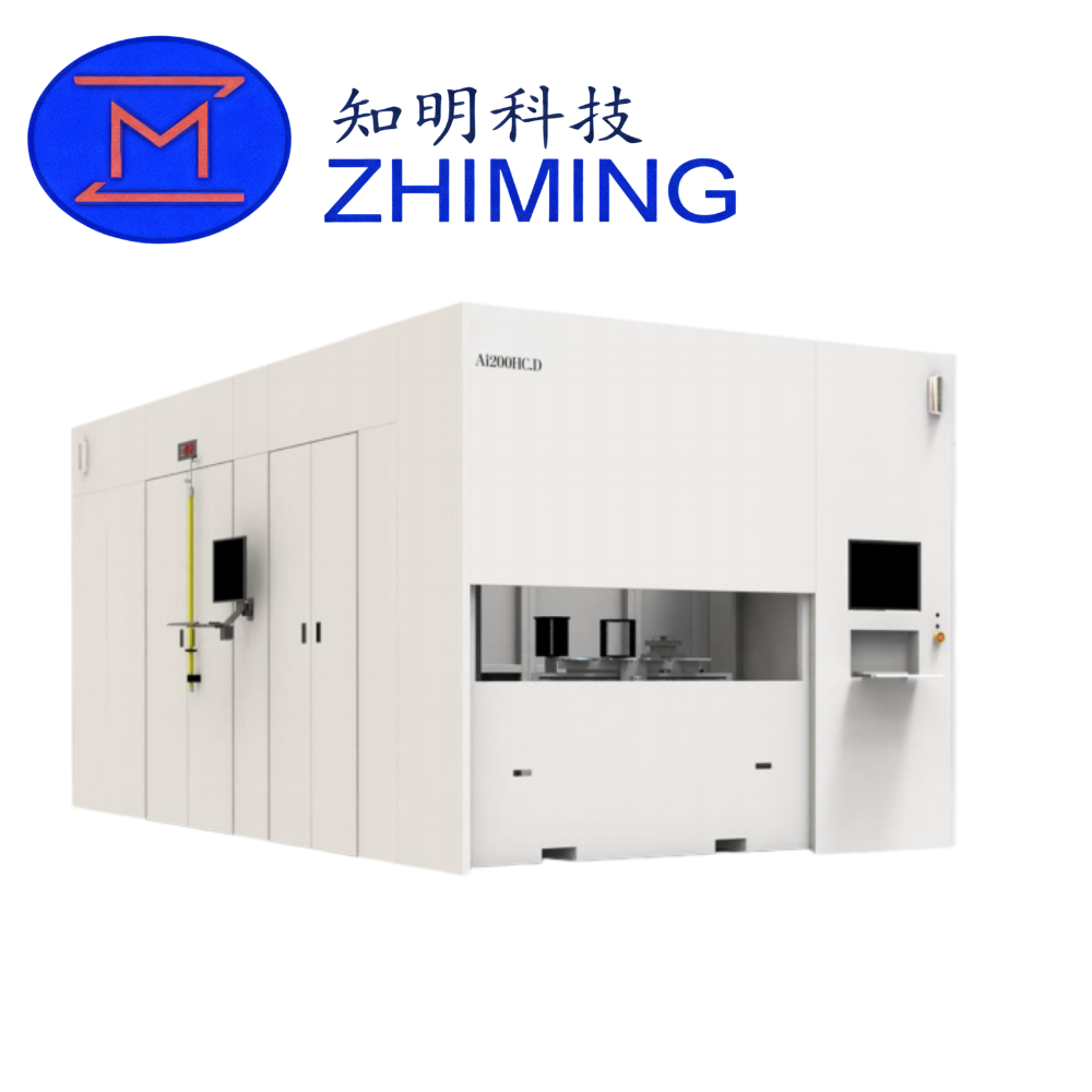
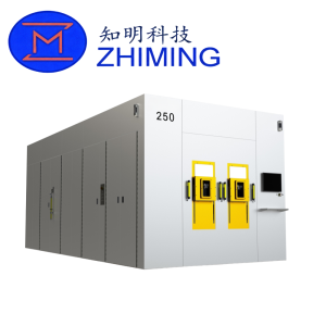
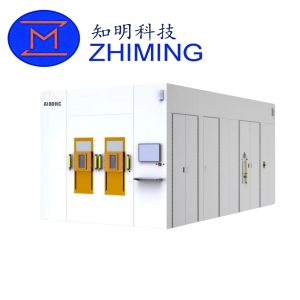
 The Ai200HC.D (High Beam) ion implantation system is designed for 6-inch and 8-inch silicon wafer semiconductor production lines. It is a high current ion implanter developed for precision doping and advanced process applications in integrated circuit manufacturing.
The system supports an energy range from 5 keV to 180 keV, providing stable beam performance and high process repeatability. It is suitable for silicon-based semiconductor manufacturing and advanced wafer bonding related processes, including Smart Cut technology integration.
Features
High Beam Stability Performance
The system maintains stable ion beam output with controlled fluctuation, ensuring consistent implantation quality during continuous production.
Wide Process Compatibility
Compatible with silicon-based processes and Smart Cut related applications, supporting advanced wafer engineering requirements.
High Precision Implant Control
Provides accurate implantation performance with:
- Angle accuracy ≤ 0.2°
- Beam parallelism ≤ 0.3°
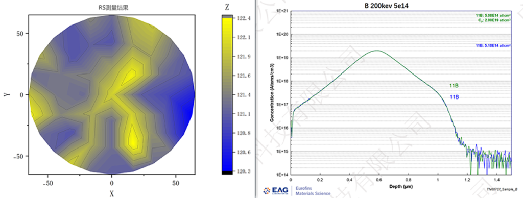
- Uniformity ≤ 1%
- Repeatability ≤ 1%
High Throughput Capability
Supports ≥ 220 wafers per hour, suitable for medium to high volume semiconductor production environments.
Batch Target Processing Capability
Supports batch target processing, improving process flexibility and enabling integration with advanced silicon wafer manufacturing technologies.
ข้อมูลจำเพาะหลัก
Process Parameters
| รายการ | ข้อกำหนด |
|---|---|
| ขนาดเวเฟอร์ | 6–8 inch silicon wafers |
| Energy Range | 5–180 keV |
| Implanted Elements | B+, BF2+, P+, As+, N+, H+ |
| Dose Range | 5E11–1E17 ions/cm² |
Beam Performance
| รายการ | ข้อกำหนด |
|---|---|
| Beam Stability | ≤ 10% per hour |
| Beam Parallelism | ≤ 0.3° |
Implantation Accuracy
| รายการ | ข้อกำหนด |
|---|---|
| Implant Angle Range | -11° to 11° |
| Angle Accuracy | ≤ 0.2° |
| Uniformity (1σ) | ≤ 1% (B+, 2E14, 150 keV) |
| Repeatability (1σ) | ≤ 1% (B+, 2E14, 150 keV) |
System Performance
| รายการ | ข้อกำหนด |
|---|---|
| ปริมาณงาน | ≥ 220 wafers per hour |
| Equipment Size | 5930 × 3000 × 2630 mm |
การสมัคร
Silicon-Based Semiconductor Manufacturing
Used in CMOS and advanced logic device fabrication, supporting precise dopant implantation processes.
Smart Cut Process Integration
Suitable for wafer bonding and layer transfer processes based on Smart Cut technology requirements.
Advanced Wafer Engineering
Applied in silicon wafer modification, structural optimization, and device performance enhancement.
Integrated Circuit Production
Supports medium-to-high volume IC manufacturing with stable process control and high throughput capability.
คำถามที่พบบ่อย
1. What wafer sizes does the Ai200HC.D support
The system supports 6-inch and 8-inch silicon wafers and is suitable for mainstream semiconductor manufacturing processes.
2. What is the energy range of this system
The energy range is 5 keV to 180 keV, supporting a wide range of implantation applications in silicon-based semiconductor devices.
3. What special process capabilities does this system support
The system is compatible with silicon-based processes and Smart Cut technology, supporting batch target processing and advanced wafer engineering applications.
รีวิว
ยังไม่มีบทวิจารณ์