
With the rapid growth of AI computing, 5G/6G communications, and high-frequency RF applications, traditional silicon-based interconnects (TSV) are increasingly limited by signal loss, thermal stress, and cost constraints. Against this backdrop, Through Glass Via (TGV) technology is emerging as a key breakthrough in advanced semiconductor packaging.
TGV enables vertical electrical interconnection by forming and metallizing microvias in ultra-thin glass substrates. It is widely considered a core enabling technology for 2.5D/3D packaging and Chiplet architectures.
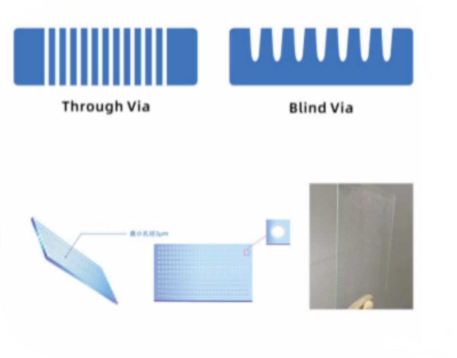
1. What is TGV (Through Glass Via)?
TGV refers to the process of creating micron-scale vertical vias (10–50 μm) in ultra-thin glass substrates (100–700 μm) such as borosilicate glass or fused silica, followed by metallization (typically copper filling) to form conductive pathways.
It replaces traditional TSV (Through Silicon Via) interposers and offers advantages such as:
- Lower signal loss
- Reduced thermal stress
- Lower manufacturing cost
- Better high-frequency performance
2. Core Working Principle
A typical TGV structure consists of:
- Glass substrate (dielectric carrier)
- Vertical microvia structure
- Metal-filled conductive vias (Copper)
These structures enable high-density vertical interconnects between chips or modules, particularly suited for high-speed and high-frequency signal transmission.
3. Standard TGV Process Flow
1) Substrate Preparation
- Cleaning and drying
- Photoresist coating / lithography
- Removal of surface contaminants
2) Laser Via Drilling (Key Process)
Ultrafast laser processing (picosecond or femtosecond lasers) is used to modify internal glass structures:
- Induces microcracks or modified zones
- Forms high aspect-ratio via channels
- Achieves via diameters down to 3 μm
- Aspect ratio up to 150:1
- Via uniformity > 95%
This is the most critical step in TGV manufacturing.
3) Wet Etching and Cleaning
- HF/BHF chemical etching
- Removal of laser-modified regions
- Smoothing via sidewalls
- Precise diameter control
- Contaminant removal
4) Metallization (Critical Step)
(1) Seed Layer Deposition
- Sputtering Ti/Cu or AlN/Cu layers
- Ensures adhesion and conductivity
(2) Copper Electroplating
- Pulse or DC electroplating
- Void-free via filling
(3) Surface Planarization
- Chemical Mechanical Polishing (CMP)
- Anti-oxidation surface treatment
5) Redistribution Layer (RDL) and Bumping
- Ultra-fine RDL wiring
- Line/space down to ≤2 μm
- Multi-layer routing (up to 6 RDL layers)
- Copper pillars or solder bumps for bonding
6) Testing and Dicing
- Electrical testing
- Wafer dicing
- Final inspection and packaging
4. Comparison of Main Via Formation Technologies
| Technology | Advantages | Disadvantages | Applications |
|---|---|---|---|
| Ultrafast laser + wet etching | High precision, 3–10 μm vias, high aspect ratio, excellent uniformity | High equipment cost, complex process | AI chips, HBM, RF applications |
| Direct laser drilling | Low cost, high speed | Rough sidewalls, low aspect ratio (<20:1) | Large vias, low-frequency use |
| Dry etching (RIE/ICP) | High precision, vertical sidewalls | Slow, expensive | Ultra-small vias (<5 μm) |
5. Glass-Based PVD Metallization Technology
In TGV manufacturing, glass-based PVD coating technology plays a critical supporting role in achieving reliable interconnect structures.
Process Features
- In-house semiconductor-grade PVD sputtering
- High-adhesion copper deposition
- Maximum copper thickness up to 10 μm
- Excellent thickness uniformity
- Low warpage and high flatness
Material Advantages
- High hardness
- Excellent wear resistance
- Strong corrosion resistance
- Stable chemical properties
- Long lifetime coating performance
6. Key Advantages of TGV Technology
Compared with traditional TSV technology, TGV offers:
- Lower signal transmission loss (ideal for high-frequency applications)
- Reduced thermal stress (better CTE matching of glass)
- Lower manufacturing cost potential
- High dimensional stability
- Better suitability for dense interconnect architectures
7. Application Areas
TGV technology is rapidly expanding into:
- AI computing chip packaging
- High-bandwidth memory (HBM)
- 5G/6G RF front-end modules
- Silicon photonics and optical interconnect (CPO)
- Chiplet heterogeneous integration
- High-speed data center interconnects
8. Industry Outlook
As advanced packaging continues evolving toward higher density, lower power consumption, and higher frequency operation, TGV is becoming a foundational technology for:
Post-Moore era 3D interconnect architectures
Future development trends include:
- Sub-5 μm via structures
- Higher-density RDL integration
- Improved mass production consistency
- Deep integration with Chiplet-based systems
Conclusion
TGV (Through Glass Via) technology is emerging as a next-generation interconnect solution due to its high-frequency performance, low thermal stress, and cost efficiency.
Its key breakthroughs lie in:
- Ultrafast laser via formation
- Void-free copper electroplating
- Ultra-fine multi-layer RDL routing
With commercial-scale adoption expected in the coming years, TGV will play a critical role in enabling AI computing and high-speed communication systems.