
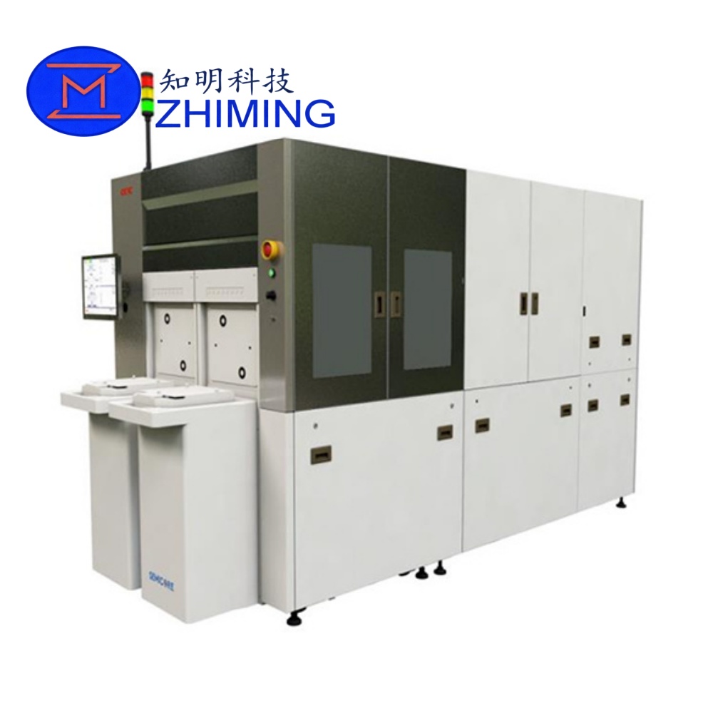
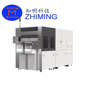
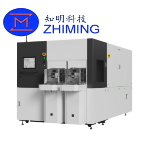
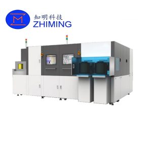
 The WG-1281 Fully Automatic Wafer Back Grinding Machine is an advanced wafer thinning solution engineered for high-precision semiconductor manufacturing. Designed to meet the increasing demand for thinner wafers in power electronics and advanced packaging, this system integrates precision mechanics, intelligent automation, and contamination-controlled design.
With support for wafers up to 12 inches, the WG-1281 is particularly well-suited for IGBT wafer thinning processes, where thickness uniformity, low stress, and minimal breakage are critical to final device performance. Its dual-spindle, three-chuck configuration ensures high throughput while maintaining excellent process stability.
In modern semiconductor production, wafer thinning is a crucial step that directly impacts device reliability, thermal performance, and packaging efficiency. The WG-1281 is built to address these challenges with a focus on precision, repeatability, and yield improvement.
Technical Features
1. Advanced X-Axis Spindle Movement
The WG-1281 incorporates an innovative X-axis spindle movement system, allowing flexible grinding path control. This feature enhances process adaptability, especially for complex wafer structures such as IGBT devices, ensuring uniform material removal across the wafer surface.
2. High-Precision Non-Contact CCD Alignment
Equipped with a non-contact CCD-based wafer alignment system, the machine accurately detects wafer positioning and optimizes grinding paths. This minimizes human intervention while significantly improving alignment precision and overall process consistency.
3. Automatic Chuck Tilt Compensation
The system automatically adjusts the tilt angle of the chuck to compensate for wafer misalignment. This reduces calibration time, shortens downtime, and ensures stable grinding quality throughout extended production cycles.
4. Low-Stress Grinding Mechanism
Unlike conventional grinding systems, the WG-1281 avoids applying external pressure to the wafer edge during processing. This low-stress approach effectively reduces wafer warpage, prevents micro-cracks, and enhances mechanical strength, which is particularly important for thin and brittle wafers.
5. Anti-Metal Contamination Design
To meet stringent semiconductor cleanliness standards, the equipment features a contamination-controlled structure that minimizes metallic particle generation. This design contributes directly to improved device yield and reliability.
6. Fully Automated Operation
The WG-1281 integrates automatic wafer transfer and cleaning systems, enabling seamless operation within automated production lines. It is compatible with modern fab environments and supports high-volume manufacturing requirements.
 애플리케이션
The WG-1281 is widely used in semiconductor back-end processing and is particularly suitable for:
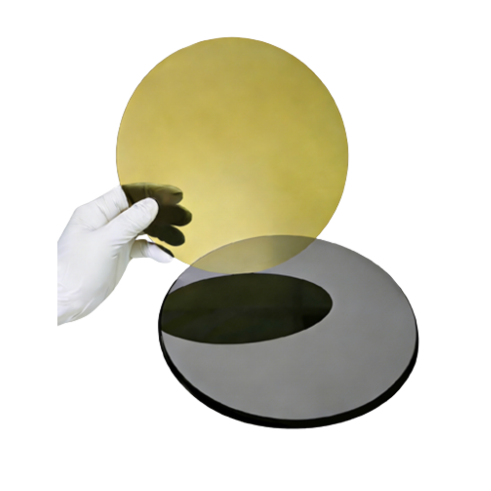
- IGBT wafer thinning (≤ 12 inches)
- Power semiconductor device manufacturing
- Silicon (Si) wafer thinning
- Silicon carbide (SiC) wafer processing
- Advanced packaging and 3D integration processes
Its versatility makes it an ideal solution for both traditional silicon-based devices and emerging wide bandgap semiconductor materials.
기술 사양
| 매개변수 | 사양 |
|---|---|
| Structure | 2 Spindles / 3 Chucks / 1 Workstation / Automatic Transfer & Cleaning System |
| 웨이퍼 크기 | 8 inch / 12 inch |
| Spindle Power | 5.5 kW / 9 kW (Optional) |
| Spindle Speed | 1000 – 6000 rpm |
| Z-axis Stroke | 120 mm |
| Z-axis Resolution | 0.1 μm |
| Chuck Type | Porous Ceramic Vacuum Chuck |
| Chuck Quantity | 3 Sets |
| Chuck Speed | 0 – 300 rpm |
| Thickness Variation (TTV) | ≤ 4 μm |
| Surface Roughness (Ra) | ≤ 0.02 μm |
| Dimensions (W×D×H) | 1450 × 3800 × 1900 mm |
| Weight | Approx. 4700 kg |
Performance Advantages
The WG-1281 delivers measurable improvements across key semiconductor manufacturing metrics:
- High Thickness Uniformity
Ensures consistent wafer thickness, improving downstream process stability. - Reduced Breakage Rate
Low-stress grinding minimizes edge chipping and wafer cracking. - Improved Yield
Anti-contamination design and precise control contribute to higher device yield. - Enhanced Process Efficiency
Automation reduces manual handling and increases throughput. - Excellent Surface Quality
Achieves ultra-low surface roughness, supporting high-performance device fabrication.
 Engineering Reliability & Industry Relevance
With the rapid evolution of power electronics and electric vehicle technologies, demand for high-quality wafer thinning equipment continues to grow. The WG-1281 is developed based on real industry requirements, focusing on:
- Stability under continuous operation
- Compatibility with high-volume manufacturing
- Adaptability to advanced materials such as SiC
- Reduction of total cost of ownership (TCO)
Its design reflects practical engineering experience combined with an in-depth understanding of semiconductor process challenges, making it a reliable choice for manufacturers seeking long-term performance.
자주 묻는 질문
1. What types of wafers can the WG-1281 process?
The WG-1281 supports a variety of wafer materials, including silicon (Si), silicon carbide (SiC), and other semiconductor substrates up to 12 inches.
2. Is the machine suitable for IGBT wafer thinning?
Yes, the WG-1281 is specifically optimized for IGBT grinding processes, ensuring low stress, high precision, and minimal wafer damage.
3. How does the machine reduce wafer breakage?
It uses a low-stress grinding method that avoids applying pressure to the wafer edge, combined with precise alignment and stable chuck control.
4. Does the equipment support automated production lines?
Yes, it includes automatic wafer transfer and cleaning systems, making it fully compatible with modern automated semiconductor fabs.
5. What is the achievable surface quality after grinding?
The WG-1281 can achieve a surface roughness of ≤ 0.02 μm, meeting high-end semiconductor manufacturing requirements.
상품평
아직 상품평이 없습니다.