
As advanced packaging moves toward thinner wafers, higher-density interconnects, backside processing, HBM, chiplets and 2.5D/3D integration, temporary wafer bonding and debonding has become an increasingly important part of semiconductor manufacturing.
A 300mm device wafer that has been thinned to tens of micrometers can no longer maintain sufficient mechanical rigidity by itself. During backgrinding, lithography, etching, deposition, TSV reveal or backside metallization, the wafer may bend, warp, crack or suffer edge damage.
A temporary carrier wafer provides mechanical support throughout these processes.
However, selecting the carrier is not simply a question of choosing glass, sapphire or silicon. The carrier material directly affects:
- Total thickness variation (TTV)
- Bow and warp
- Thermal stress
- Alignment
- Tool compatibility
- Laser transmission
- Debonding method
- Wafer breakage risk
- Carrier reuse
- Final process yield
Recent work presented at CSTIC 2026 also highlights the importance of carrier TTV, adhesive uniformity and bonding conditions in controlling the final thickness uniformity of temporarily bonded wafers.
For engineers and buyers sourcing 300mm temporary carrier wafers, the right material should therefore be selected as part of the complete bonding, thinning and debonding process.
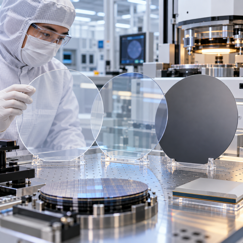
Why 300mm Thin Wafers Need a Temporary Carrier
A standard 300mm silicon wafer is relatively rigid at conventional wafer thicknesses.
After aggressive backside thinning, however, the mechanical behavior changes dramatically.
Ultra-thin wafers can experience:
- Excessive bow
- Local warpage
- Edge chipping
- Cracking
- Wafer folding
- Robot handling failures
- Non-uniform grinding
- Lithography focus problems
The thinner the wafer becomes, the more difficult it is to maintain stable handling and flatness.
Temporary bonding solves this problem by attaching the device wafer to a mechanically rigid carrier before thinning.
A typical process may include:
Device Wafer → Temporary Bonding → Backgrinding → CMP / Backside Processing → TSV / RDL / Metallization → Debonding → Cleaning
Commercial temporary-bonding systems already use rigid carriers specifically to reduce cracking, edge chipping and warpage during 300mm backside processing.
The Three Main Carrier Materials
Three carrier materials are commonly considered for advanced temporary bonding:
- Glass
- Sapphire
- Silicon
There is no universally “best” carrier.
The correct choice depends on:
- Device wafer material
- Final wafer thickness
- Process temperature
- Bonding adhesive
- Debonding technology
- Laser wavelength
- Tool configuration
- CTE matching
- Required rigidity
- Cost and reuse strategy
1. Glass Carrier Wafers
Glass is one of the most established carrier materials for temporary wafer bonding.
Its biggest advantage is optical transparency.
Depending on the glass composition, light can pass through the carrier during:
- Optical alignment
- Bond-interface inspection
- UV curing
- Laser debonding
- Defect inspection
This makes glass particularly attractive for processes in which the bonding or release layer must be activated through the carrier.
Advantages of Glass Carriers
Key benefits include:
- Good optical transparency
- Low TTV capability
- Controlled CTE
- Good surface quality
- Compatibility with laser debonding
- Availability in 200mm and 300mm formats
- Compatibility with wafer- and panel-level packaging
Specialized semiconductor glass compositions can also be engineered with different thermal-expansion characteristics. Commercial carrier solutions are available across a relatively broad CTE range, allowing the glass to be better matched to different package structures.
Limitations of Glass
Glass is still a brittle material.
Potential concerns include:
- Edge chipping
- Breakage during handling
- Scratch sensitivity
- Differences in rigidity between glass grades
- Equipment detection problems due to transparency
- Thermal mismatch if the wrong glass composition is selected
For this reason, specifying only “300mm glass carrier” is usually not enough.
The exact glass grade, thickness, TTV, CTE and optical requirements should also be defined.
2. Sapphire Carrier Wafers
Sapphire is increasingly interesting for processes that require a combination of:
- High mechanical rigidity
- High hardness
- Excellent chemical durability
- Optical transparency
- Repeated carrier reuse
Sapphire is single-crystal aluminum oxide rather than conventional glass.
Its mechanical stiffness and excellent wear resistance can make it attractive for demanding carrier applications.
Advantages of Sapphire Carriers
Typical benefits include:
- Very high hardness
- Strong mechanical stability
- Excellent wear resistance
- Good chemical resistance
- Broad optical transmission
- High-temperature stability
- Potential for repeated reuse
For processes involving repeated cleaning, handling or aggressive environments, sapphire can provide stronger long-term surface durability than many conventional glass carriers.
Where Sapphire Can Be Useful
Sapphire may be considered for:
- High-stability thin-wafer processing
- Optical through-carrier processes
- Repeated-use carrier systems
- Harsh chemical environments
- Processes requiring high mechanical rigidity
- Specialty compound semiconductor wafers
However, sapphire is not automatically the correct choice simply because it is mechanically stronger.
The high stiffness of sapphire means that thermal mismatch must be carefully controlled. A rigid carrier can transfer stress into the adhesive layer or device wafer when the carrier and device material expand differently.
Crystal Orientation Matters
Unlike ordinary glass, sapphire is a single crystal.
Therefore, the specification may also need to define:
- Crystal orientation
- Surface finish
- Optical transmission direction
- Thermal expansion direction
This becomes especially important when the temporary-bonding process involves repeated thermal cycling.
3. Silicon Carrier Wafers
Silicon is another important carrier option, particularly when the device wafer itself is silicon.
Its strongest advantage is material compatibility with existing semiconductor manufacturing infrastructure.
Advantages of Silicon Carriers
Silicon carriers generally provide:
- Similar thermal expansion to silicon device wafers
- Standard semiconductor wafer geometry
- Compatibility with wafer robots
- Compatibility with vacuum chucks
- Compatibility with electrostatic chucks
- Familiar edge and notch geometry
- Established 200mm and 300mm supply chains
When both the carrier and device wafer are silicon, thermal mismatch can be significantly reduced compared with some dissimilar-material combinations.
This can help reduce thermally induced stress during:
- Adhesive curing
- Thermal processing
- Deposition
- Annealing
- Cooling
- Debonding
Limitations of Silicon
The main disadvantage is optical opacity in the visible and UV regions.
This means conventional UV through-carrier debonding cannot normally be used.
Specialized IR debonding processes can overcome this limitation by using wavelengths that can transmit through silicon under suitable conditions.
Silicon carriers are therefore particularly attractive when:
- Existing tools are designed for silicon
- CTE matching is critical
- Visible transparency is unnecessary
- IR debonding is available
- Standard fab handling compatibility is a priority
Sapphire vs Glass vs Silicon
The basic selection logic can be summarized as follows:
| Selection Factor | Glass Carrier | Sapphire Carrier | Silicon Carrier |
|---|---|---|---|
| Optical transparency | Excellent, depending on grade | Excellent over a broad range | Limited mainly to suitable IR wavelengths |
| Mechanical rigidity | Moderate to high | Very high | High |
| Wear resistance | Moderate | Excellent | Moderate |
| CTE flexibility | Can be tailored by glass composition | Orientation-dependent | Excellent match to silicon |
| UV laser debonding | Common | Potentially suitable | Generally unsuitable |
| IR debonding | Possible | Possible | Possible with suitable IR system |
| Fab tool compatibility | May require adjustment | May require adjustment | Very good |
| Chemical durability | Grade-dependent | Excellent | Good with compatible chemistry |
| Machining cost | Moderate | Higher | Moderate |
| Reuse potential | Moderate to high | High | Process-dependent |
The carrier should therefore be chosen according to the complete process flow rather than a single property.
TTV: One of the Most Critical Carrier Specifications
Total Thickness Variation (TTV) describes the difference between the maximum and minimum thickness measured across a wafer.
In temporary bonding, poor carrier TTV can directly affect:
- Bond-line thickness
- Backgrinding uniformity
- Lithography focus
- TSV reveal
- Final thin-wafer thickness
- Wafer handling stability
A carrier that looks flat may still have excessive thickness variation.
For advanced packaging, both the carrier wafer and the adhesive layer contribute to final stack TTV.
Research presented in 2026 demonstrated that improving carrier TTV together with adhesive uniformity and bonding conditions significantly reduced both post-bonding and post-thinning TTV.
This means buyers should not evaluate carrier TTV independently from the bonding process.
Important TTV-Related Factors
Engineers should consider:
- Carrier TTV
- Device wafer TTV
- Adhesive thickness uniformity
- Bond pressure uniformity
- Chuck flatness
- Grinding tool condition
- Bonding cushion characteristics
For precision backside processing, small variations can eventually become yield problems.
CTE Matching and Thermal Stress
The coefficient of thermal expansion (CTE) is another critical parameter.
During thermal processing, the carrier and device wafer expand and contract.
If their CTE values are significantly different, the bonded stack can develop mechanical stress.
Potential consequences include:
- Bow
- Warpage
- Adhesive shear stress
- Edge delamination
- Alignment drift
- Wafer cracking
This is especially important for:
- High-temperature processing
- Multiple thermal cycles
- Large 300mm wafers
- Ultra-thin device wafers
- Fine-pitch lithography
- Hybrid bonding preparation
Glass provides flexibility because compositions with different CTE values can be selected. Silicon is attractive when bonding to silicon because the materials are naturally well matched. Sapphire requires consideration of both crystal orientation and the device material.
Bow and Warpage Control
Bow and warp become increasingly important as the device wafer becomes thinner.
A bonded 300mm stack must remain sufficiently flat for:
- Robot handling
- Vacuum chucking
- Lithography
- Etching
- Deposition
- Inspection
- CMP
Excessive warpage may prevent the wafer from entering certain process tools altogether.
Carrier-induced warpage can result from:
- CTE mismatch
- Adhesive shrinkage
- Uneven bonding pressure
- Carrier TTV
- Device wafer stress
- Non-uniform thinning
- Thermal gradients
Commercial advanced-packaging glass carriers, for example, are specifically engineered around warpage control as well as thickness and surface uniformity.
The carrier should therefore be evaluated as part of the full bonded stack.
Match the Carrier to the Debonding Process
Debonding method is often one of the strongest factors determining which carrier should be selected.
UV or Laser Debonding
If a laser must pass through the carrier to activate a release layer, carrier transmission at the selected wavelength is essential.
Glass is commonly used because it can provide good UV or visible transmission.
Sapphire may also support through-carrier laser processing, depending on:
- Sapphire thickness
- Crystal orientation
- Surface condition
- Laser wavelength
- Release-layer design
Simply specifying “transparent carrier” is not sufficient.
The actual laser wavelength should always be included in the RFQ.
IR Laser Debonding
Specialized IR debonding processes can also be used.
This is particularly important for silicon carriers because silicon can transmit selected infrared wavelengths even though it is opaque in the visible range.
Thermal Debonding
Thermal debonding typically softens or changes the temporary adhesive so that the carrier can be separated.
Important considerations include:
- Release temperature
- Device temperature limit
- Carrier CTE
- Adhesive stability
- Mechanical force during separation
Mechanical Debonding
Mechanical debonding must be carefully controlled for ultra-thin wafers.
Excessive peeling or bending can cause:
- Cracks
- Delamination
- Die damage
- Low-k damage
- Edge failure
Chemical Debonding
Chemical release requires compatibility among:
- Carrier
- Adhesive
- Release layer
- Solvent
- Device materials
Residue removal after debonding should also be considered early in the process design.
Equipment Compatibility Is Often Overlooked
A technically suitable carrier may still cause production problems if it is incompatible with existing equipment.
Important questions include:
- Can the robot detect the carrier?
- Can the chuck hold transparent wafers?
- Is an edge grip required?
- Is backside coating needed?
- Does the aligner recognize the notch?
- Is the carrier electrically conductive?
- Can the inspection system focus through the carrier?
- Does the debonding equipment support the chosen material?
Silicon often provides the easiest integration into standard silicon wafer fabs.
Transparent glass and sapphire carriers may require additional equipment configuration.
Recommended RFQ Information
When requesting a quotation for a 300mm temporary carrier wafer, provide more than just material and diameter.
A useful RFQ should include:
Carrier Material:
Glass / Sapphire / Silicon
Diameter:
300mm
Thickness:
Required nominal thickness and tolerance
TTV:
Maximum acceptable value
Bow / Warp:
Maximum limits
Surface Finish:
Single-side or double-side polished
Surface Roughness:
If required
Edge Profile:
Standard semiconductor edge or custom profile
Notch:
Required geometry
Crystal Orientation:
For silicon or sapphire
Device Wafer Material:
Silicon / SiC / GaN / glass / other
Device Wafer Final Thickness:
For example, 100 μm, 75 μm, 50 μm or thinner
Maximum Process Temperature:
Required thermal exposure
Bonding Adhesive:
If already selected
Debonding Method:
UV laser / IR laser / thermal / mechanical / chemical
Laser Wavelength:
If laser debonding is used
Cleaning Chemistry:
Required chemical compatibility
Reuse Requirement:
Single-use or multiple cycles
Quantity:
Prototype and expected production volume
Which Carrier Should You Choose?
Choose Glass When:
- Through-carrier optical access is required
- UV or laser debonding is planned
- Tunable CTE is important
- Fan-out or advanced packaging is involved
- Low TTV and optical inspection are priorities
Choose Sapphire When:
- Very high mechanical rigidity is required
- Excellent wear resistance is important
- Repeated carrier reuse is expected
- Harsh chemical environments are involved
- Optical transparency and high durability are needed together
Choose Silicon When:
- The device wafer is silicon
- Existing fab tools are optimized for silicon
- Thermal expansion matching is critical
- Visible transparency is unnecessary
- IR debonding is available
Do Not Select the Carrier by Unit Price Alone
The cheapest carrier wafer does not always create the lowest process cost.
A better evaluation should consider:
- Device wafer breakage
- Warpage
- Grinding yield
- TTV after thinning
- Debonding yield
- Cleaning cost
- Carrier reuse cycles
- Equipment modification
- Process throughput
For example, a more expensive sapphire carrier may be justified in a specialty process if its durability allows repeated reuse.
Likewise, a specially engineered glass carrier may provide a lower total process cost if it reduces warpage and enables reliable laser debonding.
Conclusion
Selecting the right 300mm temporary carrier wafer requires balancing mechanical, thermal, optical and equipment requirements.
Glass offers excellent optical access and flexible CTE options, making it especially useful for laser debonding and advanced packaging.
Sapphire provides exceptional hardness, rigidity and chemical durability, making it attractive for demanding or reusable carrier applications.
Silicon offers excellent compatibility with existing semiconductor equipment and strong thermal matching with silicon device wafers.
The most important specifications are not only carrier material and diameter, but also:
TTV, CTE, bow, warp, surface condition, device wafer thickness, process temperature and debonding method.
Carrier wafer, bonding adhesive, release layer and debonding equipment should therefore be evaluated as one integrated process system.
For custom 300mm glass, sapphire or silicon carrier wafers, providing the device wafer material, final thickness, process temperature, TTV requirement and debonding method at the RFQ stage can significantly improve technical evaluation and quotation accuracy.