
As advanced packaging moves toward HBM, chiplets, 2.5D/3D integration, TSV, backside power delivery and thinner device structures, 300mm wafers are increasingly being thinned far below conventional handling thicknesses.
Once a wafer has been background to 100 μm, 75 μm, 50 μm or even thinner, it can no longer be treated like a standard rigid silicon wafer.
Mechanical rigidity decreases dramatically, while sensitivity to:
- Warpage
- Edge chipping
- Cracking
- Vacuum chuck stress
- Robot handling
- Thermal cycling
- Debonding force
- Cleaning pressure
increases significantly.
Recent industry demonstrations have shown temporary-bonding process flows for 300mm wafers thinned to approximately 15 μm, using silicon carriers, high-temperature temporary bonding materials and IR laser debonding. This illustrates how thin-wafer handling is becoming a critical process capability for next-generation packaging.
This article explains the main process challenges after backgrinding and how carrier bonding, warpage control, edge protection, debonding and cleaning should be considered as one integrated thin-wafer handling strategy.
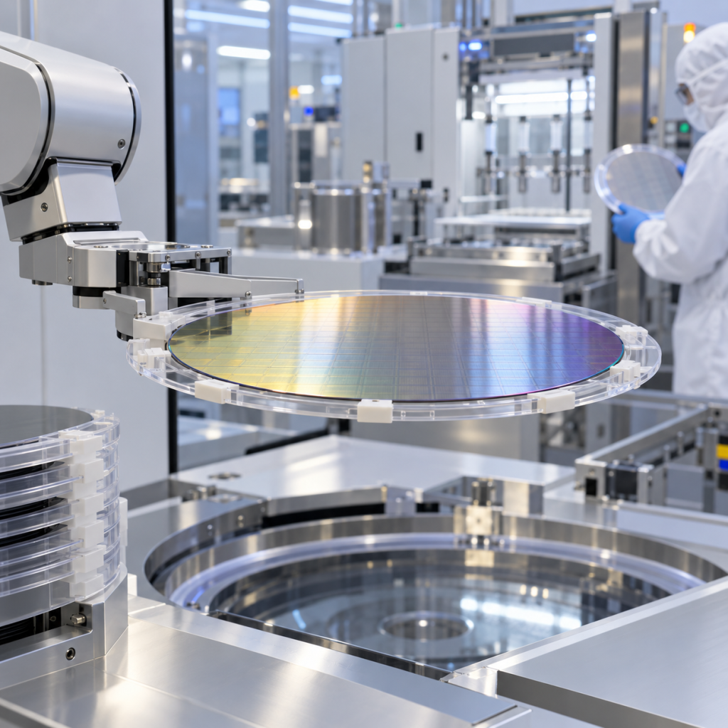
Why Backgrinding Changes Wafer Handling
Before thinning, a standard 300mm silicon wafer has enough rigidity to be handled using conventional:
- Wafer robots
- Vacuum chucks
- Cassette systems
- Metrology tools
- Cleaning equipment
After backgrinding, the wafer becomes much more flexible.
A thin wafer can deform under its own weight or under relatively small external forces.
Common problems include:
- Excessive bow
- Local warpage
- Wafer sagging
- Edge cracking
- Wafer breakage
- Vacuum-induced deformation
- Robot handling instability
- Process non-uniformity
The thinner the wafer becomes, the less safe it is to handle without external mechanical support.
For this reason, advanced packaging flows typically use temporary carrier bonding before aggressive thinning.
1. Carrier Bonding Before Backgrinding
Temporary bonding attaches the device wafer to a rigid carrier using a removable bonding material.
The carrier helps maintain mechanical stability during:
- Backgrinding
- CMP
- Backside lithography
- Dry etching
- Wet etching
- Plating
- Deposition
- TSV reveal
- Backside metallization
Temporary bonding materials must survive the thermal, chemical and mechanical stresses encountered during these processes while still allowing controlled separation at the end.
Brewer Science notes that the temporary bond must withstand stress caused by thermal cycling, CTE mismatch and deposited layers while remaining removable after processing.
Common Carrier Materials
Carrier wafers may be made from:
- Glass
- Silicon
- Sapphire
- Specialty engineered substrates
Carrier selection depends on:
- Debonding method
- Process temperature
- CTE matching
- Optical transparency
- Rigidity
- Chemical compatibility
- Reuse requirements
The important point is that the carrier is not simply a mechanical plate. It becomes part of the complete process stack.
2. Post-Backgrinding TTV Must Be Controlled
After backgrinding, total thickness variation (TTV) becomes an important parameter.
Poor TTV can affect:
- Subsequent lithography
- TSV reveal
- Backside alignment
- CMP
- Wafer bonding
- Final die thickness
- Packaging yield
TTV is influenced by more than the grinder itself.
Important contributors include:
- Carrier wafer TTV
- Bonding adhesive thickness
- Bonding pressure uniformity
- Wafer chuck flatness
- Grinding wheel condition
- Device wafer geometry
Commercial temporary-support systems report post-backgrinding TTV values around the low-micrometer range for 300mm wafers under optimized process conditions, illustrating the importance of controlling the full bonded stack rather than only the grinding step.
For high-density advanced packaging, even relatively small thickness differences may affect downstream alignment or bonding processes.
3. Warpage Becomes More Critical as Wafers Get Thinner
One of the biggest challenges after thinning is warpage.
Thin wafers are highly sensitive to stress created by:
- Frontside films
- Backside films
- Copper layers
- Redistribution layers
- Temporary adhesives
- Temperature changes
- CTE mismatch
A wafer may appear relatively flat before thinning but develop significant bow or local distortion once its thickness is reduced.
Why Warpage Matters
Excessive warpage can cause problems with:
- Robot pickup
- Vacuum chucking
- Lithography focus
- CMP uniformity
- Inspection
- Wafer bonding
- Carrier debonding
Automated debonding equipment now specifically advertises the ability to handle thinned, bowed and warped wafers up to 300mm, highlighting how important warped-wafer handling has become in production.
4. Control CTE Mismatch
The coefficient of thermal expansion, or CTE, of the device wafer, carrier and bonding material should be considered together.
During thermal processing:
- The carrier expands.
- The device wafer expands.
- The adhesive responds mechanically.
- The entire bonded stack accumulates stress.
If expansion behavior is poorly matched, the wafer can develop:
- Bow
- Warp
- Delamination
- Adhesive failure
- Edge stress
- Cracks
This is particularly important for 300mm substrates because dimensional changes accumulate over a much larger diameter than on smaller wafers.
CTE matching becomes even more important when processing:
- Silicon
- SiC
- GaN
- Glass
- Compound semiconductor substrates
on carrier materials with different thermal behavior.
5. Edge Chipping Can Become a Major Yield Problem
Wafer edges are especially vulnerable during thinning.
A conventional wafer edge is designed for normal wafer thickness. Once the wafer is aggressively ground from the backside, the original bevel geometry can become mechanically vulnerable.
Potential failures include:
- Edge chipping
- Radial cracks
- Microcracks
- Fragmentation during grinding
- Cracking during debonding
One common solution is wafer edge trimming.
Brewer Science describes edge trimming or edge recessing of approximately 0.5–1.0 mm as a technique used to reduce susceptibility to cracking and chipping after thinning.
Edge Trimming Can Help Reduce
- Backgrinding edge damage
- Crack initiation
- Particle generation
- Wafer breakage
However, the trimming depth and geometry should be coordinated with:
- Final wafer thickness
- Edge exclusion
- Device layout
- Grinding process
- Dicing strategy
6. Avoid Handling an Ultra-Thin Wafer Unsupported
After thinning, an ultra-thin wafer should ideally never become freely unsupported during transfer.
Removing the rigid carrier without first providing another support structure can expose the wafer to severe mechanical stress.
A common process sequence is:
Carrier-Bonded Wafer → Backside Processing → Film Frame Mounting → Debonding → Cleaning
Film-frame mounting allows the thin device wafer to remain supported after carrier removal.
Temporary-bonding process guidance specifically recommends supporting the thinned wafer on a film frame before carrier removal rather than allowing it to become free-standing.
This becomes increasingly important as final wafer thickness decreases.
7. Debonding Method Determines Mechanical Risk
Temporary bonding is only successful if the carrier can later be removed without damaging the device wafer.
Common debonding technologies include:
- Laser debonding
- IR laser debonding
- UV laser debonding
- Mechanical debonding
- Thermal slide-off
- Low-temperature debonding
- Chemical release
Each method creates a different stress profile.
Laser Debonding
Laser debonding uses light energy to modify or decompose a release layer.
Its main advantage for ultra-thin wafers is that separation can occur with very low mechanical force.
This is especially useful for fragile:
- Thin silicon wafers
- Compound semiconductor wafers
- Reconstituted wafers
- Fan-out structures
Modern temporary bonding systems increasingly use UV and IR laser approaches specifically to enable ultra-thin chip and advanced-packaging processes.
IR Debonding with Silicon Carriers
Silicon carriers are attractive because of their mechanical compatibility with silicon device wafers.
The challenge is that silicon is not transparent to visible or UV wavelengths.
IR laser debonding provides another route.
A recent 300mm ultrathin wafer demonstration used:
- Silicon carrier
- High-temperature temporary bond material
- IR laser debonding
to support wafers thinned to approximately 15 μm.
This makes IR debonding particularly interesting for advanced silicon wafer processing.
Mechanical Debonding
Mechanical separation can also be used with compatible temporary bonding systems.
However, peel force and bending stress must be carefully controlled.
For ultra-thin wafers, excessive mechanical load can cause:
- Wafer fracture
- Delamination
- Device damage
- Edge cracking
Low-force mechanical debonding therefore requires both suitable bonding materials and well-controlled equipment.
8. Debonding Equipment Must Handle Warped Wafers
Thin-wafer debonders are increasingly becoming integrated process systems rather than simple carrier-removal tools.
Modern automated equipment may combine:
- Debonding
- Film-frame support
- Thin-wafer handling
- Warped-wafer handling
- Cleaning
- Recipe control
- Process monitoring
For example, EVG’s automated 300mm debonding platform combines carrier separation, wafer cleaning and thin-wafer handling while supporting bowed and warped substrates.
This integration reduces the number of times an unsupported thin wafer must be moved between machines.
9. Adhesive Residue Must Be Removed After Debonding
Carrier removal does not always complete the process.
Temporary bonding materials or release layers can remain on the device wafer.
Residual material may interfere with:
- Wafer inspection
- Subsequent bonding
- Metallization
- Dicing
- Assembly
- Surface metrology
For this reason, post-debond cleaning is an important part of the process.
Cleaning Requirements
Cleaning should remove:
- Temporary adhesive
- Release-layer residues
- Organic contamination
- Particles
without damaging:
- Metal structures
- RDL
- Passivation
- Low-k materials
- Exposed device surfaces
10. Wet Cleaning Can Reduce Mechanical Stress
For fragile thin wafers, wet chemical cleaning can be preferable to aggressive mechanical cleaning.
Some temporary bonding systems allow solvent-based cleaning while the wafer remains mounted on a film frame.
This minimizes mechanical loading on the thinned wafer.
Brewer Science describes spray cleaning with wet chemistries after debonding and notes that solvent-based cleaning can remove temporary bonding residues while avoiding significant mechanical stress on the thin wafer.
11. Carrier Cleaning and Reuse
The carrier itself may also need cleaning after debonding.
Potential residues include:
- Adhesive
- Release material
- Deposition contamination
- Etch residues
- Particles
Depending on the carrier material and process, carriers may be cleaned and reused.
Carrier reuse can reduce:
- Material cost
- Waste
- Cost per wafer
However, reuse requires inspection.
Important parameters include:
- Surface scratches
- Edge chips
- TTV
- Flatness
- Residual contamination
- Surface roughness
A carrier that has accumulated scratches or particles may introduce new defects into later bonding cycles.
12. Cleaning Chemistry Must Match the Device Stack
A cleaning process should never be selected based only on how effectively it removes adhesive.
The chemistry must also be compatible with:
- Cu
- Al
- Ni
- RDL polymers
- Passivation
- Low-k dielectric
- Si
- SiC
- GaN
- Glass
Potential cleaning failures include:
- Metal corrosion
- Polymer swelling
- Surface staining
- Particle redeposition
- Residual organic films
Before volume production, cleaning chemistry should therefore be qualified using the actual device stack.
13. Thin-Wafer Handling Equipment Must Be Evaluated as a System
Handling ultra-thin wafers requires more than upgrading one machine.
The complete process flow should be reviewed.
Relevant equipment includes:
- Temporary bonders
- Backgrinders
- CMP tools
- Edge trimmers
- Wet benches
- Plating equipment
- Lithography tools
- Inspection systems
- Debonders
- Film-frame mounters
- Cleaning tools
- Wafer robots
Each system should be checked for its ability to process:
- Thin wafers
- Carrier-bonded stacks
- Warped substrates
- Transparent carriers
- Non-standard substrate thicknesses
Recommended Process Flow
A typical ultra-thin 300mm process may follow:
1. Device wafer inspection
↓
2. Edge trimming if required
↓
3. Temporary adhesive coating
↓
4. Carrier wafer bonding
↓
5. Backgrinding
↓
6. CMP / fine grinding
↓
7. Backside processing
↓
8. Warpage and TTV inspection
↓
9. Film-frame mounting
↓
10. Carrier debonding
↓
11. Adhesive residue cleaning
↓
12. Final inspection
↓
13. Dicing / downstream assembly
The exact sequence depends on the packaging architecture.
Specifications Engineers Should Monitor
For thin-wafer handling, key parameters include:
Device Wafer
- Diameter
- Initial thickness
- Final thickness
- TTV
- Bow
- Warp
Carrier Wafer
- Material
- Thickness
- TTV
- Flatness
- CTE
- Surface finish
Bonding
- Adhesive thickness
- Bond uniformity
- Void level
- Maximum process temperature
Backgrinding
- Target thickness
- Grinding TTV
- Edge condition
- Surface damage
Debonding
- Debond method
- Laser wavelength
- Maximum force
- Device wafer support
Cleaning
- Residue level
- Chemical compatibility
- Particle cleanliness
- Surface condition
Common Failure Modes
Several common problems should be investigated during process development.
Wafer Cracking After Grinding
Possible causes:
- Excessive edge damage
- Poor carrier support
- Grinding stress
- Wafer bow
Excessive Warpage
Possible causes:
- CTE mismatch
- Film stress
- Adhesive shrinkage
- Non-uniform bonding
Edge Chipping
Possible causes:
- Incorrect edge geometry
- Insufficient edge trimming
- Grinding vibration
Debonding Fracture
Possible causes:
- Excessive mechanical force
- Poor release layer
- Unsupported thin wafer
High Residue After Cleaning
Possible causes:
- Incompatible adhesive
- Insufficient cleaning chemistry
- Excessive thermal exposure
Each problem should be investigated across the entire stack rather than blaming only one processing step.
Why This Matters for HBM and Advanced Packaging
Ultra-thin wafer handling is becoming increasingly important because advanced packages require thinner devices and more complex backside processing.
Applications include:
- HBM
- 3D IC
- 2.5D interposers
- TSV
- Fan-out wafer-level packaging
- Chiplets
- Power semiconductor devices
Temporary bonding/debonding is increasingly treated as a foundational process module because it maintains wafer geometry throughout thinning, RDL build-up, plating, molding and wet processing. This is particularly important as warpage increasingly limits overlay and assembly yield.
RFQ Checklist for Ultra-Thin Wafer Projects
When discussing a thin-wafer process with a carrier or equipment supplier, provide:
Wafer Diameter:
200mm / 300mm
Device Material:
Si / SiC / GaN / other
Initial Thickness:
Before grinding
Target Thickness:
After grinding
Carrier Material:
Glass / silicon / sapphire
Carrier Thickness
Carrier TTV
Maximum Bow / Warp
Maximum Process Temperature
Temporary Bonding Material
Backside Process:
CMP / TSV / plating / deposition / other
Debonding Method:
UV / IR / thermal / mechanical
Cleaning Chemistry
Final Surface Requirement
Prototype Quantity
Expected Production Volume
This information helps suppliers evaluate both carrier wafer requirements and process compatibility.
Conclusion
Handling an ultra-thin 300mm wafer after backgrinding is not simply a wafer transportation problem.
It requires coordinated control of:
Carrier Bonding → Backgrinding → TTV → Warpage → Edge Integrity → Film-Frame Support → Debonding → Cleaning
As wafers become thinner, small amounts of mechanical or thermal stress can translate into significant wafer deformation or breakage.
Temporary carrier bonding provides the mechanical support needed during grinding and backside processing. Edge trimming can reduce chipping risk. Controlled debonding minimizes stress during carrier removal, while compatible cleaning processes remove adhesive residues without damaging fragile device structures.
For advanced packaging projects involving thin 200mm or 300mm wafers, defining the complete process flow—including the carrier, adhesive, grinding target, debonding technology and cleaning requirements—at the beginning of development can significantly reduce manufacturing risk and improve yield.