
Semiconductor and advanced-material wafers are increasingly required in non-standard diameters.
A development program may have a 300 mm silicon wafer but require 200 mm samples for an existing process tool. A glass wafer may need to be converted into several smaller round substrates. Sapphire or SiC material may need to be cored from a larger wafer or plate because the required diameter is not readily available as a standard commercial wafer.
These requirements are commonly described as:
- wafer resizing;
- wafer downsizing;
- wafer cutdown;
- wafer coring;
- diameter conversion; or
- custom wafer machining.
Although these terms are sometimes used interchangeably, the manufacturing requirements can be very different.
Reducing a wafer diameter is not simply a matter of cutting a circle.
For semiconductor processing, the finished wafer may still need controlled:
- diameter tolerance;
- roundness;
- flat or notch orientation;
- edge bevel;
- edge chipping;
- thickness;
- TTV;
- bow and warp;
- front-surface protection;
- cleanliness; and
- compatibility with automated wafer-handling equipment.
These factors become especially important for 200 mm and 300 mm silicon, glass, sapphire and SiC wafers, where both the material value and downstream processing cost can be high.
This guide explains the major wafer resizing and coring options and the information engineers should include when requesting a quotation.
What Is Wafer Resizing?
Wafer resizing means converting an existing wafer or substrate to a smaller external diameter or different geometry.
A typical example is:
300 mm wafer → 200 mm wafer
or:
200 mm wafer → 150 mm wafer
The original wafer may be:
- silicon;
- SOI;
- fused silica;
- borosilicate glass;
- sapphire;
- SiC;
- compound semiconductor material; or
- another specialty substrate.
After the outer material is removed, the newly generated circumference normally requires additional edge finishing.
Depending on the final application, this may include:
rough cut → diameter finishing → edge grinding → bevel/chamfer → notch or flat machining → cleaning → dimensional inspection
The finished product may therefore look similar to a standard wafer even though it was produced from a larger parent substrate.
What Is Wafer Coring?
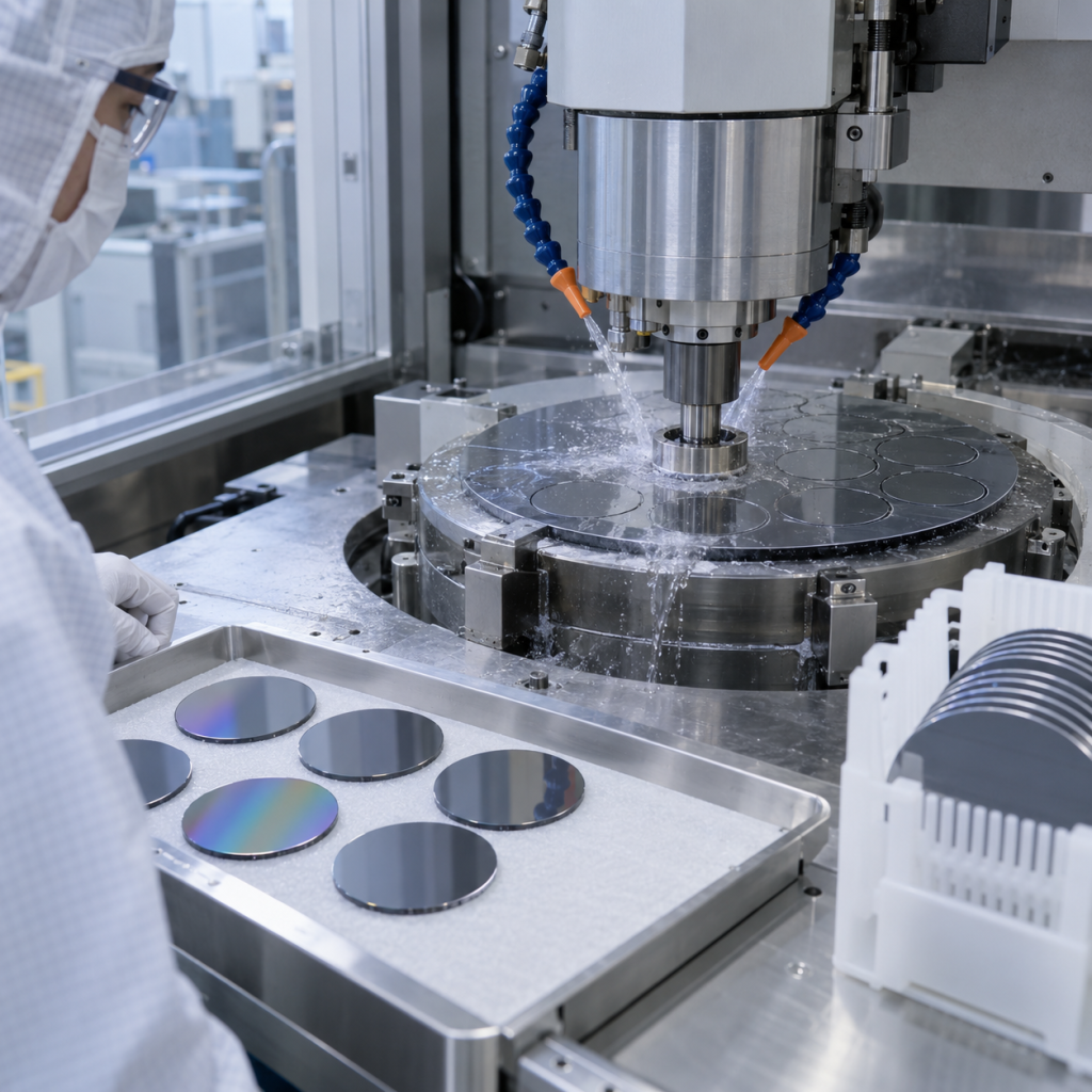
Wafer coring is related to resizing but normally refers to extracting one or more circular substrates from a larger wafer, plate or panel.
For example:
300 mm glass wafer → multiple 50 mm circular substrates
or:
large sapphire plate → several custom-diameter sapphire wafers
Instead of preserving the center of the original wafer and removing only its circumference, coring can select specific locations within the parent material.
This makes wafer coring useful when:
- only a small amount of expensive material is required;
- several test wafers are needed from one large substrate;
- particular areas of the parent wafer must be selected;
- a non-standard wafer diameter is required;
- R&D equipment accepts smaller wafers;
- valuable deposited films must be reused;
- customer-provided material needs to be converted to another format.
Coring can therefore improve material utilization, particularly for expensive materials such as sapphire and SiC.
Wafer Resizing vs Wafer Coring
| Parameter | Wafer Resizing | Wafer Coring |
|---|---|---|
| Typical purpose | Reduce complete wafer diameter | Extract smaller circular wafers |
| Original wafer center | Usually retained | May or may not be retained |
| Number of output wafers | Usually one | Potentially multiple |
| Flat/notch preservation | Often possible | Usually needs new reference feature |
| Typical example | 300 mm → 200 mm | 300 mm → multiple 50 mm wafers |
| Material utilization | Moderate | Potentially high |
| Common applications | Tool compatibility, wafer reuse | R&D samples, specialty substrates |
The correct process therefore depends on whether the customer requires one resized wafer or multiple cored wafers.
Why Resize a 300mm Wafer to 200mm?
A common reason is equipment compatibility.
A customer may obtain material in 300 mm format, but the available:
- lithography tool;
- bonding tool;
- grinder;
- CMP tool;
- coating system;
- metrology system;
- epitaxy reactor; or
- laboratory fixture
may accept only 200 mm wafers.
Replacing the equipment can be far more expensive than resizing the wafer.
Another common situation occurs during R&D.
A customer may purchase a large wafer containing a specialized:
- thin film;
- epitaxial layer;
- dielectric coating;
- metal film;
- SOI structure;
- SiC layer;
- optical coating.
Smaller wafers can then be extracted for process trials.
Commercial wafer processors already offer downsizing of 200 mm and 300 mm wafers, and low-stress coring or laser cutdown is used specifically to convert existing wafers to smaller formats.
1. Diameter Tolerance: The First Critical Specification
One of the first questions in any wafer-resizing project should be:
What finished diameter and tolerance are actually required?
For example:
Ø200.00 mm ± 0.20 mm
is very different from:
Ø200.00 mm ± 0.05 mm
Tighter tolerances generally require additional finishing and inspection.
Diameter matters because an oversized wafer may:
- fail to enter a cassette;
- interfere with end effectors;
- contact chamber hardware;
- create alignment errors.
An undersized wafer can also create problems with:
- edge sensors;
- centering algorithms;
- robot handling;
- vacuum chucks.
SEMI’s current diameter-measurement guidance specifically notes that semiconductor wafer diameter must meet the applicable SEMI M1 limits or other mutually agreed limits so the wafer can fit process equipment correctly.
Do Not Automatically Apply Silicon Tolerances to Other Materials
This is particularly important.
SEMI M1 applies specifically to polished single-crystal silicon wafers. It can provide useful dimensional guidance, but glass, sapphire and SiC wafers should be specified according to the actual process and customer agreement rather than assuming identical tolerances.
In 2024, SEMI published a revision changing the specified diameter tolerance for 300 mm polished silicon wafers from ±0.20 mm to ±0.10 mm, reflecting tighter industry requirements.
That does not mean every resized 300 mm glass, sapphire or SiC wafer should automatically be specified at ±0.10 mm.
Custom resizing capability depends on:
- material;
- wafer thickness;
- cutting method;
- edge-finishing method;
- final diameter;
- surface protection;
- quantity.
For example, one commercial laser cutdown process reports achievable diameter tolerance down to approximately 0.05 mm under its specified process conditions, while its water-guided laser process lists approximately ±0.20 mm. These numbers demonstrate why the required tolerance should be agreed during RFQ rather than assumed from the nominal diameter alone.
2. Roundness Is Different from Diameter
A wafer can meet a diameter measurement at one point while still being slightly non-circular.
This is why roundness can become important for precision applications.
Possible deviations include:
- ovality;
- localized edge irregularity;
- flat-to-diameter variation;
- machining marks;
- local edge defects.
SEMI’s wafer-diameter measurement guide notes that measurements made at only a limited number of positions do not completely characterize wafer roundness.
Therefore, if roundness is critical for:
- automated handling;
- precision bonding;
- rotating stages;
- optical fixtures; or
- high-accuracy metrology,
the RFQ should explicitly state a roundness requirement rather than specifying diameter alone.
3. Why Edge Bevel Is Necessary After Resizing
After a wafer is cut to a new diameter, the newly generated edge is often sharp.
A sharp edge creates several risks:
- chipping;
- crack initiation;
- reduced wafer strength;
- particle generation;
- damage during cassette loading;
- breakage during vacuum handling.
For this reason, semiconductor wafers usually have an engineered edge profile rather than a perfectly square 90° edge.
The finishing process may be called:
- edge rounding;
- edge beveling;
- edge grinding;
- chamfering.
Commercial wafer-downsizing services specifically use post-cutdown edge rounding because it reduces the probability of edge cracking and chipping.
4. Edge Bevel vs Chamfer
The terminology varies between manufacturers.
A bevel or rounded wafer edge generally transitions gradually from the front surface to the outer circumference and then toward the backside.
A chamfer is more commonly understood as a straight angled surface.
For semiconductor-grade wafers, controlled rounded profiles are often preferred because they reduce stress concentration and particle generation.
SEMI documentation has specifically noted that constant-radius profiles with blended front- and backside transitions are preferred for manufacturability and reduced particle and chip generation.
For custom glass, sapphire and SiC parts, however, a customer may deliberately request a chamfer instead.
The drawing should therefore specify whether the edge requires:
rounded bevel / chamfer / polished edge / ground edge / custom profile
rather than simply stating “finished edge.”
5. Edge Chipping: One of the Main Yield Risks
Edge chipping is one of the most important quality issues in wafer resizing.
During cutting or grinding, brittle materials can develop small fractures along the circumference.
Typical defects include:
- front-side chips;
- backside chips;
- lateral cracks;
- subsurface cracks;
- microfractures;
- notch-area chipping.
A visible edge chip is not only cosmetic.
It can become the starting point of catastrophic wafer breakage during:
- spin coating;
- CMP;
- thermal cycling;
- grinding;
- bonding;
- vacuum handling;
- high-speed rotation.
DISCO notes that wafer-edge chipping can reduce mechanical strength and lead to wafer breakage.
This is particularly important when resizing sapphire and SiC, because both are hard, brittle materials.
6. Why Thin Wafers Need More Care
Wafer thickness strongly affects resizing risk.
A standard-thickness wafer may tolerate edge processing relatively well.
An ultra-thin wafer can be much more fragile.
When a conventional rounded wafer is thinned significantly, the original edge geometry can effectively become sharper and mechanically weaker. Under grinding water and processing forces, this region can flutter and develop edge chipping, potentially leading to wafer breakage.
For thin-wafer resizing, additional information should therefore be supplied:
- current wafer thickness;
- final target thickness;
- whether resizing occurs before or after thinning;
- temporary carrier condition;
- front-side device protection;
- allowable backside contact.
In many projects it may be safer to resize before aggressive thinning.
7. Silicon Wafer Resizing
Silicon is generally the most mature material for wafer downsizing.
Typical processing options can include:
- laser cutdown;
- water-guided laser cutting;
- mechanical coring;
- edge grinding;
- beveling;
- lapping;
- polishing.
Silicon is particularly suitable for projects such as:
300 mm → 200 mm
200 mm → 150 mm
150 mm → 100 mm
Potential applications include:
- equipment compatibility;
- wafer reclaim;
- test wafers;
- SOI development;
- coated wafer reuse;
- university and R&D programs.
One important issue is whether the parent wafer already contains devices.
If it does, the cutting process must consider:
- particle contamination;
- heat-affected regions;
- cooling fluid;
- front-side protection;
- film delamination.
Some laser resizing processes use vacuum extraction and protective photoresist to reduce contamination of the existing wafer surface during cutdown.
8. Glass Wafer Resizing and Coring
Glass behaves differently from silicon.
Depending on the application, the material may be:
- fused silica;
- quartz glass;
- borosilicate glass;
- BF33 / BOROFLOAT-type glass;
- alkali-free glass;
- optical glass;
- TGV glass substrate.
Glass wafer coring is particularly useful for:
- MEMS;
- anodic bonding;
- microfluidics;
- optical devices;
- advanced packaging;
- TGV process development.
The main quality concerns include:
- edge chipping;
- radial cracks;
- surface scratches;
- contamination;
- thickness variation;
- edge stress.
Glass also presents an advantage: because it can be transparent, positioning relative to existing structures may be easier in certain machining setups.
However, the process needs to consider whether the wafer already contains:
- TGV holes;
- metal routing;
- thin films;
- cavities;
- patterned structures.
These features can alter local stress during coring.
9. Sapphire Wafer Resizing
Sapphire presents greater machining difficulty because of its:
- high hardness;
- brittle fracture behavior;
- crystallographic anisotropy.
The RFQ should specify the sapphire orientation, for example:
- C-plane (0001);
- A-plane;
- R-plane;
- M-plane;
- custom orientation.
Orientation becomes particularly important if the resized wafer requires a new flat or notch.
A new orientation feature should not simply be placed visually.
Its relationship to the crystallographic axis must be specified if that orientation matters to the customer’s downstream process.
For precision sapphire resizing, customers should therefore provide:
orientation + off-cut + flat/notch direction + diameter + thickness
Large sapphire wafers are also commercially discussed with custom edge geometries and protective chamfers, illustrating the importance of edge design as substrate diameter increases.
10. SiC Wafer Resizing
SiC presents similar but often even more demanding machining challenges.
Important variables include:
- 4H-SiC or 6H-SiC;
- conductive or semi-insulating material;
- Si-face or C-face;
- crystal orientation;
- off-axis angle;
- wafer thickness;
- existing epitaxy.
The most common commercial device substrate is 4H-SiC, and the material may carry a valuable epitaxial layer.
When resizing an epi wafer, process development must therefore protect:
- epitaxial surface;
- edge exclusion region;
- device structures;
- backside metallization.
Because SiC is hard and brittle, the required edge geometry should be planned together with the cutting process rather than added as an afterthought.
11. What Happens to the Original Flat or Notch?
This is an important RFQ question.
When a wafer is simply reduced concentrically, the original notch may be removed.
There are then several possible solutions.
Option A — Create a New Notch
A new notch can be machined at the required orientation.
Option B — Create a Flat
A flat can be added instead if the downstream equipment supports it.
Option C — No Orientation Feature
Some laboratory applications do not require a notch or flat.
Option D — Preserve Orientation Relative to the Original Wafer
During resizing, the original notch or flat can be used as a reference so that the crystallographic orientation is maintained when the new orientation feature is created.
Commercial laser cutdown processes specifically use the original flat or notch as a reference and can re-cut orientation features after resizing.
For semiconductor substrates, this is much safer than asking:
Please add one notch.
The RFQ should specify the orientation of the notch relative to the crystal axis.
12. Surface Protection During Coring
A finished wafer may already have a high-value polished or patterned surface.
During resizing, three main risks are:
Particle Contamination
Cutting generates debris.
Surface Scratching
Handling and fixturing can damage polished surfaces.
Chemical or Thermal Damage
Some cutting methods introduce water, heat or protective coatings.
Depending on the substrate, protection may include:
- protective film;
- photoresist;
- dicing tape;
- temporary bonding;
- non-contact front-side handling;
- vacuum debris collection.
The required method should depend on the existing device or film structure.
13. Should Resizing Be Done Before or After Polishing?
Whenever possible, this should be considered during process planning.
A simplified sequence for a raw substrate might be:
coring → edge grinding → bevel → lapping → polishing → cleaning
This approach allows some machining damage to be removed during subsequent finishing.
For an already polished or patterned wafer, however, resizing obviously occurs after surface preparation.
In that case, the priority changes from removing machining damage to protecting the finished surfaces.
Therefore, a supplier needs to know whether the wafer is:
- raw;
- lapped;
- SSP;
- DSP;
- epitaxial;
- coated;
- patterned;
- device-complete.
14. TTV, Bow and Warp After Resizing
Diameter is not the only dimensional specification.
The customer may also need:
- TTV;
- bow;
- warp;
- flatness;
- parallelism.
Resizing itself does not necessarily improve these parameters.
In some situations, stress relief after removal of outer material can slightly change wafer shape.
Additional lapping or polishing may therefore be needed when the final wafer must meet tight flatness requirements.
SEMI M1 treats thickness, TTV, bow and warp as separate dimensional properties from wafer diameter, which is important when creating procurement specifications.
A good RFQ should therefore avoid statements such as:
200 mm wafer, semiconductor quality.
Instead specify the actual dimensional limits required by the process.
15. 200mm and 300mm Wafer Handling Considerations
Larger wafers make dimensional errors more consequential.
A 300 mm substrate requires consideration of:
- larger unsupported span;
- higher material value;
- increased sensitivity to bow and warp;
- robot end-effector compatibility;
- cassette geometry;
- center positioning;
- notch detection;
- edge-grip handling.
Processing systems are specifically designed around 200 mm or 300 mm formats. For example, commercial grinding systems are separately configured for Φ200 mm and Φ300 mm wafer handling.
A resized wafer that is nominally “200 mm” but lacks an appropriate edge profile or orientation feature may therefore still fail to behave like a standard 200 mm wafer in automated tools.
16. Custom Diameter Wafers
Not every project requires a SEMI-standard diameter.
Typical custom sizes may include:
- Ø25 mm;
- Ø50 mm;
- Ø75 mm;
- Ø100 mm;
- Ø120 mm;
- Ø150 mm;
- Ø200 mm;
- custom inch-based dimensions.
Custom wafer coring is particularly common for:
- university research;
- optical experiments;
- MEMS development;
- bonding tests;
- materials characterization;
- prototype semiconductor processes.
In these applications, the required diameter tolerance can often be selected according to the actual fixture rather than automatically requiring semiconductor prime-wafer tolerances.
This can substantially reduce processing difficulty and cost.
17. One Large Wafer vs Multiple Cored Wafers
For expensive materials, a coring layout can be designed to maximize usable pieces.
Suppose a customer has:
1 × 300 mm sapphire wafer
but requires small substrates for multiple experiments.
Instead of purchasing many individually grown wafers, it may be possible to extract several smaller discs from the parent wafer.
The layout should account for:
- edge exclusion;
- parent wafer notch;
- existing defects;
- patterned areas;
- saw/laser clearance;
- minimum spacing between cored wafers.
This is especially useful when the parent material contains a rare or expensive layer.
18. How Should Edge Chipping Be Specified?
Avoid specifications such as:
No chipping allowed.
For brittle materials, this can be difficult to define and inspect consistently.
A better specification is quantitative.
For example:
Maximum edge chip length: ___ µm
Maximum chip depth: ___ µm
Inspection magnification: ___×
Inspection area: full circumference
If front-side and backside chipping requirements differ, specify them separately.
This creates a measurable acceptance criterion.
19. Example RFQ — 300mm to 200mm Silicon Wafer Resizing
A useful RFQ might look like this:
Material: Silicon
Original Diameter: 300 mm
Final Diameter: 200.00 mm
Diameter Tolerance: ±0.10 mm
Thickness: 775 µm
Surface: DSP
Orientation: (100)
Original Notch: <110>
New Orientation Feature: Notch, preserve original orientation
Edge: Rounded / beveled
Front Surface: Patterned, must be protected
Maximum Edge Chip: Customer specified
Quantity: 10 pcs
Application: Equipment compatibility / process development
This allows a supplier to determine the correct resizing process much more quickly.
20. Example RFQ — Sapphire Wafer Coring
Material: Sapphire
Orientation: C-plane (0001)
Parent Wafer: Ø200 mm
Required Size: Ø50.8 mm
Thickness: 500 µm
Diameter Tolerance: ±0.10 mm
Surface: DSP
Edge: Protective bevel
Flat: Required, orientation specified
Maximum Chipping: ___ µm
Quantity: 12 pcs
Application: Optical / semiconductor R&D
21. Example RFQ — SiC Wafer Resizing
Material: 4H-SiC
Type: N-type / semi-insulating
Face: Si-face
Orientation: (0001), 4° off-axis if applicable
Original Diameter: 200 mm
Final Diameter: 150 mm
Thickness: ___ µm
Surface: Epitaxial / polished
Epi Layer: Yes / No
Backside Metal: Yes / No
Notch: Required
Edge Finish: Beveled
Quantity: ___ pcs
For SiC epi wafers, information about the epi structure and surface-protection requirement should always be provided.
22. Wafer Resizing RFQ Checklist
Before requesting a quotation, provide the following information.
Material
- Silicon
- SOI
- Glass type
- Fused silica
- Sapphire
- 4H-SiC / 6H-SiC
- Other material
Original Wafer
- Diameter
- Thickness
- Surface finish
- Orientation
- Flat/notch
- Existing coatings
- Existing devices
Required Final Wafer
- Diameter
- Diameter tolerance
- Thickness
- Quantity
Edge
- Edge bevel
- Chamfer
- Polished edge
- Maximum chipping
- Edge inspection requirement
Orientation
- Crystal orientation
- Off-cut
- New flat/notch
- Flat/notch orientation tolerance
Geometry
- TTV
- Bow
- Warp
- Flatness
Surface Protection
- SSP/DSP
- Epitaxial layer
- Patterned front side
- Backside metallization
- Protective coating allowed or not
Application
- Semiconductor processing
- Bonding
- Lithography
- Optical
- MEMS
- R&D
- Equipment compatibility
Providing these details can significantly reduce technical clarification time before quotation.
23. How to Select a Wafer Resizing Supplier
For high-value substrates, the lowest cutting price should not be the only criterion.
Important capabilities include:
Multiple Material Experience
Silicon processing knowledge does not automatically translate to sapphire or SiC.
Edge Finishing Capability
A rough-cut circle is not equivalent to a finished semiconductor wafer.
Orientation Control
The supplier should understand the relationship between crystal direction and flat/notch placement.
Surface Protection
This is essential for epitaxial, patterned or optical-quality wafers.
Dimensional Inspection
Diameter, thickness, edge condition and orientation should be measurable after processing.
Custom RFQ Support
The supplier should be able to evaluate non-standard diameters instead of restricting customers to catalog wafer sizes.
Conclusion
Wafer resizing and coring provide a practical way to convert existing silicon, glass, sapphire and SiC substrates into the dimensions required by new processes and equipment.
However, a successful wafer resizing project requires more than cutting the parent wafer to a smaller diameter.
The complete specification should consider:
material → original diameter → final diameter → tolerance → orientation → notch/flat → edge profile → chipping → surface protection → TTV → bow/warp → cleaning
For 200 mm and 300 mm semiconductor wafers, diameter and edge geometry are especially important because the finished wafer may need to operate in automated handling equipment.
For glass, sapphire and SiC, the machining method must additionally account for each material’s fracture behavior, hardness and crystal structure.
ZMSH can evaluate custom wafer resizing, coring and substrate machining requirements for silicon, glass, sapphire, SiC and other semiconductor materials. Customers can provide the parent-wafer specification, target diameter, thickness, orientation, edge requirements and quantity for technical evaluation and quotation.
FAQ
Can a 300mm wafer be resized to 200mm?
Yes. Wafer downsizing services can convert larger wafers to smaller formats, including applications involving 200 mm and 300 mm material. The exact process depends on substrate material, thickness, surface condition and required tolerance.
What is the difference between wafer resizing and wafer coring?
Wafer resizing generally reduces one complete wafer to a smaller outside diameter. Wafer coring usually extracts one or more smaller circular substrates from a larger wafer or plate.
Can the original wafer orientation be preserved after resizing?
Yes. The original flat or notch can be used as an orientation reference, after which a new flat or notch can be machined into the resized wafer.
Does a resized wafer need an edge bevel?
For many semiconductor-processing applications, yes. A properly designed rounded or beveled edge reduces stress concentration, particle generation and the risk of edge chipping.
Can sapphire and SiC wafers be resized?
Yes, but both are hard, brittle materials and generally require tighter control of cutting, edge finishing and chipping than ordinary silicon processing.
What diameter tolerance should I specify?
The tolerance should be determined by the downstream equipment and application. Do not automatically copy silicon-wafer standards for sapphire, glass or SiC. For standard silicon, the relevant current SEMI specification should be checked; custom resized wafers can also use supplier-customer agreed tolerances.