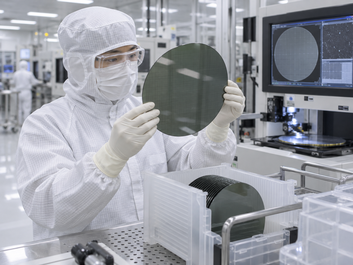
300mm Wafer Edge Metrology for Hybrid Bonding: Edge Roll-Off, TTV, Bow, Warp, Surface Particles and Overlay Yield Read More »
Industry News Ultra-Thin 300mm Wafer Handling After Backgrinding: Carrier Bonding, Warpage, Edge Chipping, Debonding and Cleaning Read More »
Industry News How to Select Carrier Wafers for 300mm Temporary Bonding: Sapphire vs Glass vs Silicon, TTV, CTE, Warpage and Debonding Read More »
Wafer Resizing and Coring for 200mm and 300mm Silicon, Glass, Sapphire and SiC: Diameter Tolerance, Edge Bevel, Chipping and RFQ Guide Read More »
Laser Dicing vs Blade Dicing for Sapphire and SiC Wafers: Chipping, Kerf Width, Yield, Throughput and Equipment Selection Read More »
Industry News SiC Epitaxial Wafer Specifications for 200mm Mass Production: Epilayer Uniformity, Doping Control, BPD Conversion, Edge Exclusion and Surface Defects Read More »
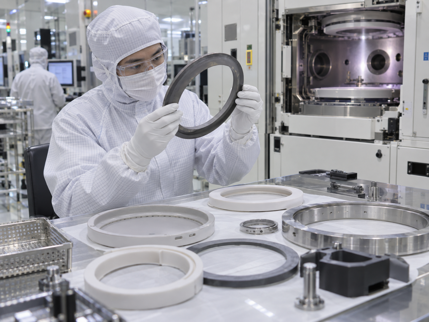
Industry News Semiconductor Wafer Consumables Lifetime Guide: Plasma Erosion, Particle Generation, Contamination, Replacement Criteria and RFQ Specifications Read More »
LNOI / TFLN Wafer Selection Guide for Integrated Photonics: X-Cut vs Z-Cut, LN Film Thickness, BOX, Handle Substrate and Surface Quality Read More »
Industry News SOI Wafer Thickness Guide: Device Layer, BOX Thickness, Handle Wafer and Selection for MEMS, RF and Silicon Photonics Read More »
Industry News Diamond-Copper Composite Heat Spreaders: Thermal Conductivity, CTE Matching and AI/HPC Packaging Applications Read More »