
In semiconductor manufacturing, wafer geometry plays a critical role in determining process stability, lithography accuracy, bonding quality, and ultimately device yield. As wafer diameters continue to increase and advanced packaging technologies become more demanding, the need for precise wafer metrology has never been greater.
Among the many parameters used to evaluate wafer quality, Total Thickness Variation (TTV) and Total Indicated Reading (TIR) are frequently encountered. Although both measurements are related to wafer thickness and flatness, they describe different physical characteristics and are often misunderstood.
This article explains the definitions, measurement methods, applications, and key differences between TIR and TTV, helping engineers better understand wafer geometry specifications.
Understanding Wafer Thickness Measurements
Semiconductor wafers are expected to have highly uniform thickness across their entire surface. Even slight variations can affect:
- Lithography focus accuracy
- Wafer handling and transport
- Wafer bonding processes
- CMP performance
- Device reliability and yield
To evaluate thickness uniformity, manufacturers use several geometric parameters, including:
- Thickness
- TTV (Total Thickness Variation)
- Bow
- Warp
- TIR (Total Indicated Reading)
Each parameter provides unique information about the wafer’s physical condition.
What Is TTV (Total Thickness Variation)?
Definition
TTV represents the difference between the maximum and minimum thickness measured across a wafer.
Mathematically:
TTV = Maximum Thickness − Minimum Thickness
TTV focuses solely on thickness uniformity and does not consider the wafer’s orientation or rotational behavior.
Measurement Principle
Thickness measurements are taken at multiple points across the wafer surface using:
- Capacitive sensors
- Optical interferometers
- Contact thickness gauges
- Laser metrology systems
The highest and lowest thickness values are identified, and their difference becomes the TTV value.
Example
If a wafer thickness ranges from:
- Maximum thickness: 726 μm
- Minimum thickness: 721 μm
Then:
TTV = 726 − 721 = 5 μm
A smaller TTV indicates better thickness uniformity.
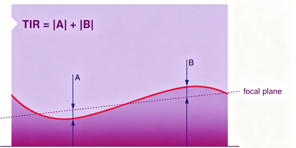
What Is TIR (Total Indicated Reading)?
Definition
TIR measures the total variation observed when a wafer is rotated around its center axis.
Unlike TTV, TIR reflects the combined influence of:
- Thickness variation
- Surface irregularities
- Wafer eccentricity
- Fixture alignment errors
- Surface runout
TIR is commonly used in precision mechanical and metrology applications.
Measurement Principle
The wafer is mounted on a spindle and rotated 360 degrees while a displacement sensor continuously records surface movement.
The difference between the highest and lowest readings during rotation is defined as:
TIR = Maximum Indicator Reading − Minimum Indicator Reading
Example
During rotation:
- Highest reading: +3 μm
- Lowest reading: −4 μm
Then:
TIR = 3 − (−4) = 7 μm
TTV vs TIR: Key Differences
| Parameter | TTV | TIR |
|---|---|---|
| Full Name | Total Thickness Variation | Total Indicated Reading |
| Primary Purpose | Thickness Uniformity | Rotational Surface Variation |
| Measures Thickness? | Yes | Partially |
| Influenced by Surface Shape? | No | Yes |
| Influenced by Wafer Eccentricity? | No | Yes |
| Requires Rotation? | No | Yes |
| Typical Application | Semiconductor Wafer Qualification | Precision Metrology and Equipment Alignment |
The most important distinction is that:
TTV measures thickness variation directly, whereas TIR measures overall positional variation during rotation.
As a result, TIR values are often larger than TTV values because additional geometric errors are included.
Relationship Between TIR and TTV
Although related, TIR and TTV are not interchangeable.
In an ideal wafer:
- Perfect centering
- Perfect spindle alignment
- No surface irregularities
TIR may approach the TTV value.
However, in real manufacturing environments, TIR is usually influenced by additional factors:
Surface Runout
Microscopic waviness or local defects can increase indicator readings.
Wafer Eccentricity
If the wafer center does not perfectly align with the spindle axis, TIR increases.
Fixture Errors
Chuck flatness and mounting accuracy can contribute to measurement variation.
Mechanical Vibrations
Equipment instability may introduce measurement noise.
Consequently:
TIR ≥ TTV in most practical situations.
Why TIR Matters in Semiconductor Manufacturing
As wafer diameters expand from 150 mm and 200 mm to 300 mm and beyond, geometric precision becomes increasingly important.
TIR measurements are commonly used in:
Wafer Grinding
Monitoring spindle accuracy during back grinding processes.
Wafer Polishing
Evaluating rotational stability during CMP operations.
Wafer Inspection Systems
Ensuring accurate positioning and focusing.
Wafer Bonding
Reducing alignment errors in advanced packaging applications.
MEMS Manufacturing
Maintaining strict flatness requirements for microelectromechanical structures.
Typical Industry Requirements
The acceptable TTV and TIR values depend on wafer type and application.
Silicon Wafers
| Diameter | Typical TTV |
| 150 mm | < 5 μm |
| 200 mm | < 3 μm |
| 300 mm | < 1 μm |
Advanced SiC Wafers
| Diameter | Typical TTV |
| 6 Inch | < 10 μm |
| 8 Inch | < 5 μm |
TIR specifications are generally determined by equipment manufacturers and process requirements rather than substrate standards alone.
TIR, TTV, Bow, and Warp: A Complete Picture
No single parameter can fully describe wafer geometry.
Engineers typically evaluate:
| Parameter | Description |
| Thickness | Average wafer thickness |
| TTV | Thickness uniformity |
| TIR | Rotational variation |
| Bow | Center displacement from reference plane |
| Warp | Overall wafer deformation |
Together, these measurements provide a comprehensive understanding of wafer quality and process compatibility.
Conclusion
TTV and TIR are both essential wafer metrology parameters, but they serve different purposes.
TTV quantifies thickness uniformity across the wafer surface, making it a critical specification for substrate manufacturers and semiconductor fabs. TIR, on the other hand, measures total positional variation during rotation and reflects the combined effects of thickness variation, surface irregularities, and mechanical alignment.
As semiconductor manufacturing continues to move toward larger wafer diameters, advanced packaging, and tighter process tolerances, understanding the distinction between TTV and TIR becomes increasingly important for engineers involved in wafer production, inspection, and device fabrication.
By accurately evaluating both parameters, manufacturers can improve process stability, equipment performance, and overall device yield.