
In semiconductor manufacturing, wafer quality is about much more than material purity. Even a perfectly grown silicon, sapphire, quartz, or silicon carbide wafer can cause production issues if its geometry is not properly controlled.
Among the most important wafer geometry parameters are TTV (Total Thickness Variation), Bow, and Warp. These measurements help engineers evaluate wafer thickness uniformity and flatness before a wafer enters critical processes such as lithography, bonding, thinning, and packaging.
This article explains what these parameters mean, why they matter, and how they are measured.
Why Wafer Flatness Matters
Modern semiconductor devices are manufactured with extremely tight tolerances. A slight variation in wafer thickness or flatness can affect:
- Photolithography focus accuracy
- Wafer bonding quality
- Thin-film deposition uniformity
- CMP (Chemical Mechanical Polishing) performance
- Dicing and packaging yield
As wafer diameters increase and device structures become more complex, controlling wafer geometry becomes increasingly important.
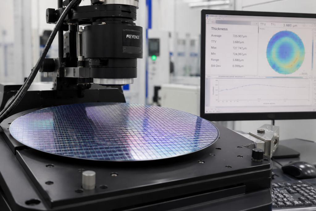
What Is TTV (Total Thickness Variation)?
TTV, or Total Thickness Variation, measures how uniform a wafer’s thickness is across its entire surface.
It is defined as the difference between the maximum and minimum thickness measured on the wafer.
Formula:
TTV = Maximum Thickness − Minimum Thickness
For example, if the thickest point on a wafer is 726 μm and the thinnest point is 721 μm, the TTV is 5 μm.
A lower TTV value generally indicates better thickness uniformity, which is essential for precision semiconductor processing.
Why TTV Is Important
Excessive TTV can lead to:
- Focus errors during lithography
- Uneven polishing results
- Poor wafer bonding performance
- Increased process variation
High-end semiconductor wafers often require TTV values of only a few microns or less.
What Is Wafer Bow?
Bow describes the overall curvature of a wafer relative to a reference plane.
Imagine placing a wafer on a flat surface. If the center of the wafer rises above or sinks below the reference plane, the wafer exhibits bow.
Bow is typically caused by internal stresses generated during:
- Epitaxial growth
- Thin-film deposition
- Thermal processing
- Wafer thinning
A positive bow means the wafer center is higher than the reference plane, while a negative bow means it is lower.
Why Bow Matters
Bow can influence:
- Wafer handling
- Alignment accuracy
- Bonding processes
- Thin-film stress evaluation
For engineered wafers and advanced substrates, bow is often monitored throughout the manufacturing process.
What Is Wafer Warp?
Warp measures the overall deformation of a free-standing wafer.
Unlike bow, which mainly describes uniform curvature, warp includes both global bending and local surface distortions.
As a result, warp usually provides a more realistic representation of a wafer’s actual shape.
Why Warp Is Important
Large warp values may cause:
- Equipment handling issues
- Vacuum chucking problems
- Reduced bonding yield
- Packaging reliability concerns
Warp has become particularly important in advanced packaging technologies, where multiple materials with different thermal expansion coefficients are combined.
Bow vs. Warp: What’s the Difference?
Although these terms are often used together, they describe different aspects of wafer geometry.
| Parameter | Bow | Warp |
|---|---|---|
| Measures | Overall curvature | Total deformation |
| Includes local distortion | No | Yes |
| Typical value | Smaller | Larger |
| Main application | Stress analysis | Packaging and bonding |
A simple way to remember the difference is:
Bow describes the wafer’s curvature, while warp describes its actual shape.
How Are TTV, Bow, and Warp Measured?
Modern wafer metrology relies primarily on non-contact optical measurement techniques.
Laser Scanning Systems
Laser-based systems scan both wafer surfaces and generate detailed thickness and flatness maps.
These systems can measure:
- Thickness
- TTV
- Bow
- Warp
They are widely used for silicon, sapphire, quartz, and SiC wafers.
Optical Profilometers
Optical profilometers create three-dimensional surface profiles with high accuracy.
They are commonly used for:
- Warp analysis
- Surface topography measurement
- Flatness inspection
White-Light Interferometers
For ultra-precision applications, white-light interferometry can provide sub-micron and even nanometer-level measurement resolution.
These systems are often used in MEMS, photonics, and research applications.
Typical Wafer Geometry Specifications
The acceptable values for TTV, bow, and warp vary depending on wafer material and application.
Typical examples include:
| Wafer Type | Typical TTV |
| Silicon Wafer | 1–5 μm |
| Sapphire Wafer | 3–10 μm |
| Quartz Wafer | 5–20 μm |
| SiC Wafer | 2–10 μm |
Actual specifications depend on wafer diameter, thickness, and end-use requirements.
Conclusion
TTV, bow, and warp are fundamental parameters used to evaluate wafer geometry and flatness.
- TTV measures thickness uniformity.
- Bow measures overall wafer curvature.
- Warp measures total wafer deformation.
As semiconductor manufacturing continues to advance, tighter control of these parameters is essential for achieving higher yields, better device performance, and improved process stability.
Whether you are sourcing silicon wafers, sapphire wafers, quartz wafers, or silicon carbide substrates, understanding TTV, bow, and warp can help you select the right wafer specifications for your application.