
As advanced semiconductor packaging moves toward thinner wafers, finer interconnect pitches, hybrid bonding, chiplet integration and three-dimensional stacking, wafer handling is becoming increasingly difficult.
A standard 200 mm or 300 mm silicon wafer is relatively rigid before thinning. Once the wafer is ground down to tens of micrometers—or even thinner—it can become extremely fragile. Bow, warp, edge cracking and handling damage can increase rapidly during backside processing, lithography, deposition, etching and bonding.
This is where temporary wafer carriers become important.
A temporary carrier provides mechanical support to the device wafer during thinning and downstream processing. After the required processes are completed, the device wafer is separated from the carrier through a controlled debonding process.
For advanced packaging applications, however, choosing a carrier is no longer simply a matter of selecting a piece of glass or silicon with the correct diameter. Carrier flatness, coefficient of thermal expansion, stiffness, surface quality, bonding chemistry, debonding method and 300 mm dimensional stability can directly affect process yield.
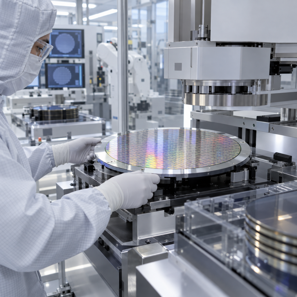
What Is a Temporary Wafer Carrier?
A temporary wafer carrier is a rigid supporting substrate temporarily bonded to a semiconductor wafer during processes in which the original wafer cannot safely support itself.
A typical temporary bonding process may follow this sequence:
Device wafer → temporary bonding → carrier wafer → wafer thinning → backside processing → inspection → debonding → cleaning → subsequent bonding or packaging
Temporary wafer bonding is particularly useful for:
- Ultra-thin silicon wafers
- 2.5D and 3D advanced packaging
- Hybrid bonding preparation
- Through-silicon-via processing
- Fan-out wafer-level packaging
- MEMS wafers
- Compound semiconductor wafers
- SiC and GaN device processing
- Backside redistribution layers
- Backside power delivery processes
Temporary bonding therefore acts primarily as a handling and process-support technology.
It is important to distinguish this from hybrid bonding itself.
Hybrid bonding creates a permanent dielectric-to-dielectric and metal-to-metal interface, typically involving Cu/SiO₂ or related structures. Temporary bonding, by contrast, holds and stabilizes a wafer during the processes required before the final permanent bond is formed.
Hybrid bonding requires exceptionally clean, planar and accurately aligned surfaces. As pitch becomes smaller, wafer distortion and local non-flatness become increasingly important process variables.
Why Temporary Carriers Matter for Hybrid Bonding
Hybrid bonding increasingly depends on aggressive wafer thinning.
For advanced logic, HBM, chiplets and 3D integration, reducing the thickness of each layer can lower total package height and shorten vertical interconnect distances.
But a very thin wafer presents several problems:
- Reduced mechanical rigidity
- Increased wafer bow
- Increased local warp
- Higher edge fracture risk
- Vacuum chuck handling difficulty
- Increased sensitivity to deposited-film stress
- Higher risk during wet processing
- Greater alignment instability
A rigid temporary carrier helps maintain the wafer’s mechanical geometry during these processes.
Temporary bonding is therefore not merely a transportation aid. It can become part of the dimensional control strategy for advanced packaging.
Recent industry work has demonstrated temporary carrier processing of 300 mm wafers thinned to approximately 15 µm, using silicon carriers, high-temperature temporary bonding materials and IR laser debonding. This illustrates how important temporary support has become as advanced packaging moves toward extremely thin substrates.
1. Flatness, Bow and Warp Requirements
Flatness is one of the most important parameters when specifying a temporary wafer carrier.
In conventional wafer specifications, engineers often focus on:
- TTV — Total Thickness Variation
- Bow
- Warp
- Global flatness
For advanced packaging and hybrid bonding, however, global bow alone may not describe the entire problem.
Local surface deformation can affect:
- Lithography focus
- Wafer-to-wafer alignment
- Bonding contact
- Copper pad coplanarity
- Overlay accuracy
- Wafer chucking
- Bond strength uniformity
Industry attention is increasingly shifting from a single global bow value toward process-dependent wafer shape and local warpage, particularly as package dimensions increase and hybrid bonding tolerances become tighter.
Carrier specifications that should be considered include:
| Parameter | Why It Matters |
|---|---|
| Diameter tolerance | Determines compatibility with handling and bonding equipment |
| Thickness | Influences rigidity and equipment compatibility |
| TTV | Affects bonded-stack thickness uniformity |
| Bow | Influences chucking and process alignment |
| Warp | Indicates overall substrate deformation |
| Surface flatness | Important for uniform temporary bonding |
| Surface roughness | Influences bonding-layer uniformity |
| Edge geometry | Reduces chipping and particle generation |
| Parallelism | Important for grinding and polishing consistency |
For demanding 300 mm applications, the carrier specification should therefore be established together with the bonding process rather than treating the carrier as an independent mechanical component.
2. Temporary Carrier Material Selection
Several materials can be used as temporary wafer carriers.
The most common options include:
Silicon Carrier Wafers
Silicon is widely used because its mechanical properties and thermal expansion behavior are close to those of conventional silicon device wafers.
Advantages include:
- Excellent semiconductor equipment compatibility
- Good dimensional stability
- Similar CTE to silicon device wafers
- High-quality wafer-grade surfaces
- Suitable for high-temperature processing
- Mature 200 mm and 300 mm supply chain
Silicon carriers can be particularly attractive when thermal mismatch between the device wafer and carrier must be minimized.
One limitation is that silicon is not transparent to visible light, which can influence the choice of optical or laser debonding process.
Glass Carrier Wafers
Glass carriers are frequently used where optical transparency is valuable.
Potential advantages include:
- Optical transparency
- Compatibility with some laser-release systems
- Adjustable glass composition and CTE
- Good surface flatness
- Availability in large wafer formats
- Easier visual inspection of bonded interfaces in some processes
However, “glass carrier” is a broad category.
Borosilicate glass, fused silica and engineered glass can have very different:
- CTE
- thermal resistance
- optical transmission
- chemical resistance
- Young’s modulus
- surface quality
The correct material must therefore be selected according to the downstream thermal and chemical process.
Sapphire Carriers
Sapphire can also be considered where high mechanical strength, thermal stability, chemical resistance or optical transparency are required.
Typical benefits include:
- High hardness
- Excellent chemical resistance
- Good thermal stability
- Optical transparency over a broad spectral range
- High mechanical strength
However, sapphire’s cost and thermal-expansion behavior must be considered carefully when it is paired with silicon or other device materials.
For some compound-semiconductor processes, sapphire may offer advantages that justify the higher material cost.
3. CTE Matching and Thermal Stress
The coefficient of thermal expansion is a critical carrier-selection parameter.
Consider a bonded stack consisting of:
Device wafer + temporary adhesive + carrier wafer
If the device wafer and carrier expand at substantially different rates during heating, stress develops across the bonded stack.
That stress can lead to:
- Bow
- Warp
- Adhesive failure
- Delamination
- Wafer cracking
- Alignment shift
- Non-uniform thickness after processing
The higher the process temperature and the larger the wafer diameter, the more important thermal-expansion mismatch becomes.
This becomes especially significant at 300 mm, because even relatively small material mismatches can produce larger absolute dimensional changes across the wafer.
Carrier material, bonding-layer modulus, bonding temperature and downstream thermal cycle therefore need to be evaluated as one system.
4. Temporary Bonding Material
The carrier alone does not determine process performance.
The temporary bonding material between the carrier and device wafer is equally important.
Depending on the process, temporary bonding layers may include:
- Thermoplastic adhesives
- Thermoset materials
- UV-release layers
- Laser-release layers
- Specialty polymer systems
- Temporary bonding tapes
Commercial automated bonding systems can support several types of adhesives and carriers, including silicon, glass and sapphire, for substrates up to 300 mm.
Important bonding-material parameters include:
Thermal Stability
The adhesive must survive the highest downstream process temperature without:
- Decomposition
- Excessive softening
- Outgassing
- Delamination
- Bond-line deformation
Some backside processes may exceed 250°C or 300°C.
Recent development work has pushed temporary bonding materials into even higher-temperature process windows. Systems demonstrated for advanced thin-wafer processing have reported compatibility with processing temperatures above 400°C before controlled laser debonding.
Topography Accommodation
Device wafers may already contain:
- Copper pillars
- Microbumps
- Redistribution layers
- Trenches
- MEMS structures
- Passivation layers
The bonding layer must accommodate this topography without creating voids or transferring excessive stress to sensitive structures.
Chemical Resistance
Temporary bonding materials must also tolerate process chemicals used during:
- Cleaning
- Etching
- Plating
- Lithography
- CMP-related processes
Failure of the bonding layer during wet processing can result in catastrophic wafer loss.
5. Debonding Methods
The ideal temporary bonding system must provide strong support during processing but allow low-stress separation afterward.
Several debonding methods are available.
Mechanical Debonding
Mechanical separation can be performed at room temperature or under controlled conditions.
Advantages can include:
- Relatively simple equipment
- No requirement for optical transparency
- Compatibility with selected polymer systems
However, mechanical force must be carefully controlled for ultra-thin wafers.
Thermal Slide-Off Debonding
The bonding layer is heated until its mechanical properties allow the carrier to slide away from the device wafer.
This technology has been used extensively in thin-wafer processing.
Potential concerns include thermal exposure and process time.
UV Debonding
UV-sensitive release materials can reduce adhesion after ultraviolet exposure.
The carrier and adhesive system must allow sufficient UV energy to reach the release layer.
Laser Debonding
Laser debonding is becoming increasingly important for advanced packaging.
A properly designed release layer absorbs laser energy at a controlled interface, enabling the carrier to be separated with very little mechanical force on the thinned device wafer.
Laser debonding can be attractive for:
- Ultra-thin wafers
- Advanced packaging
- High-value device wafers
- Processes requiring low mechanical stress
- 300 mm manufacturing
Automated debonding equipment is already designed to handle thinned, bowed and warped wafers up to 300 mm and can integrate debonding, cleaning and film-frame mounting.
6. Why 300mm Wafer Handling Is More Difficult
Scaling from 150 mm or 200 mm to 300 mm is not simply a matter of increasing carrier diameter.
A 300 mm wafer has a much larger unsupported area.
After thinning, this produces greater sensitivity to:
- Gravity-induced deformation
- Film stress
- Thermal gradients
- Vacuum chuck pressure
- Robot end-effector support
- Edge handling
- Bond-layer non-uniformity
Equipment compatibility also becomes critical.
Engineers need to confirm:
- SEMI-standard dimensions
- Carrier thickness
- Edge profile
- Robot handling compatibility
- Load-port compatibility
- Wafer identification requirements
- Backside surface condition
- Maximum acceptable stack thickness
Modern temporary bonding platforms support wafers up to 300 mm and, in some cases, oversized carrier configurations and warped-wafer handling.
7. Carrier Surface Quality
Carrier surface finish affects the quality of the temporary bond.
Important parameters may include:
Surface roughness (Ra)
A very rough surface can affect adhesive thickness and bonding uniformity.
Particles
Particles trapped between the wafer and carrier can cause local stress, void formation and thickness variation.
Scratch and dig defects
For transparent carriers and optical inspection processes, surface defects may interfere with inspection.
Flatness and TTV
Carrier thickness variation can transfer into the bonded stack and affect thinning uniformity.
Edge quality
Chipped or poorly finished edges can become particle sources during repeated handling.
Carrier cleaning and packaging therefore should be treated as part of the material specification.
8. Reusable vs Disposable Carriers
Another purchasing decision is whether the carrier will be reused.
High-quality silicon, glass and sapphire carriers can potentially support multiple process cycles when the material and cleaning sequence allow it.
Reusable carriers can reduce cost per wafer, but the supplier and user need to control:
- Surface contamination
- Adhesive residue
- Particle accumulation
- Edge damage
- Thickness change
- Surface roughness
- Flatness after repeated thermal cycles
Carrier lifetime should therefore be established using both dimensional inspection and process yield data.
9. How to Specify a Temporary Wafer Carrier
When requesting a quotation, providing only the carrier diameter is usually not sufficient.
A more useful RFQ should include:
Basic Dimensions
- Carrier material
- Diameter
- Thickness
- Diameter tolerance
- Thickness tolerance
- Quantity
Geometry
- TTV
- Bow
- Warp
- Flatness
- Parallelism
Surface
- Single-side or double-side polished
- Surface roughness
- Scratch/dig requirement if applicable
- Cleaning specification
Edge
- Edge profile
- Bevel requirement
- Edge exclusion requirement
Process Conditions
- Device wafer material
- Original wafer thickness
- Final wafer thickness after grinding
- Maximum process temperature
- Temporary adhesive type
- Bonding method
- Debonding method
- Required laser wavelength if laser debonding is used
Equipment
- 200 mm or 300 mm tool
- Bonding equipment
- Grinding equipment
- Handling system
- Film-frame requirement
Providing this information allows the carrier specification to be optimized for the actual process rather than simply supplying a generic wafer.
Temporary Wafer Carrier Selection Checklist
Before selecting a carrier, engineers should answer five questions:
- What is the device wafer material and final thickness?
- What is the maximum downstream process temperature?
- How much bow and warp can the process tolerate?
- Which temporary bonding and debonding technology will be used?
- Does the carrier need to support 200 mm or 300 mm automated handling?
For hybrid bonding applications, additional attention should be paid to wafer-shape stability because surface planarity and alignment directly influence the permanent bonding process.
Conclusion
Temporary wafer carriers are becoming an increasingly important enabling technology for advanced semiconductor packaging.
As device wafers become thinner and packaging architectures move toward hybrid bonding, HBM, chiplets and 3D integration, the carrier must provide more than basic mechanical support.
Successful carrier selection requires coordinated control of:
material → CTE → thickness → TTV → bow/warp → bonding layer → process temperature → debonding method → 300 mm handling
Silicon, glass and sapphire carriers each offer different advantages, and there is no single carrier material suitable for every process.
For demanding applications, especially ultra-thin 200 mm and 300 mm wafers, the best solution is to define the carrier together with the actual bonding, thinning, thermal and debonding process.
ZMSH can provide custom silicon, glass, sapphire and other wafer carrier substrates for semiconductor processing and advanced packaging applications. Customers can provide drawings or target specifications including wafer diameter, thickness, TTV, bow, warp, surface finish and downstream processing conditions for technical evaluation and quotation.
FAQ
What is a temporary wafer carrier used for?
A temporary wafer carrier mechanically supports a fragile or thinned semiconductor wafer during grinding, backside processing, lithography, deposition, etching and other manufacturing steps. The carrier is removed after processing.
Which material is best for a temporary wafer carrier?
Silicon, glass and sapphire can all be used. The correct choice depends on the device-wafer material, process temperature, CTE requirements, bonding chemistry and debonding method.
Can temporary wafer carriers be made for 300mm wafers?
Yes. 300 mm temporary bonding and debonding equipment is commercially available, and 300 mm carrier systems are widely investigated and used for advanced packaging and ultra-thin-wafer processing.
What parameters should be included in a wafer carrier RFQ?
The most useful parameters include material, diameter, thickness, TTV, bow, warp, surface roughness, polishing condition, edge profile, operating temperature, device wafer material, bonding adhesive and debonding method.
Can a temporary wafer carrier be reused?
Potentially yes. Reuse depends on the carrier material, adhesive-removal process, cleaning method, surface condition, contamination level and dimensional stability after repeated process cycles.